Enhancing SEM Performance with Ion Milling Technology
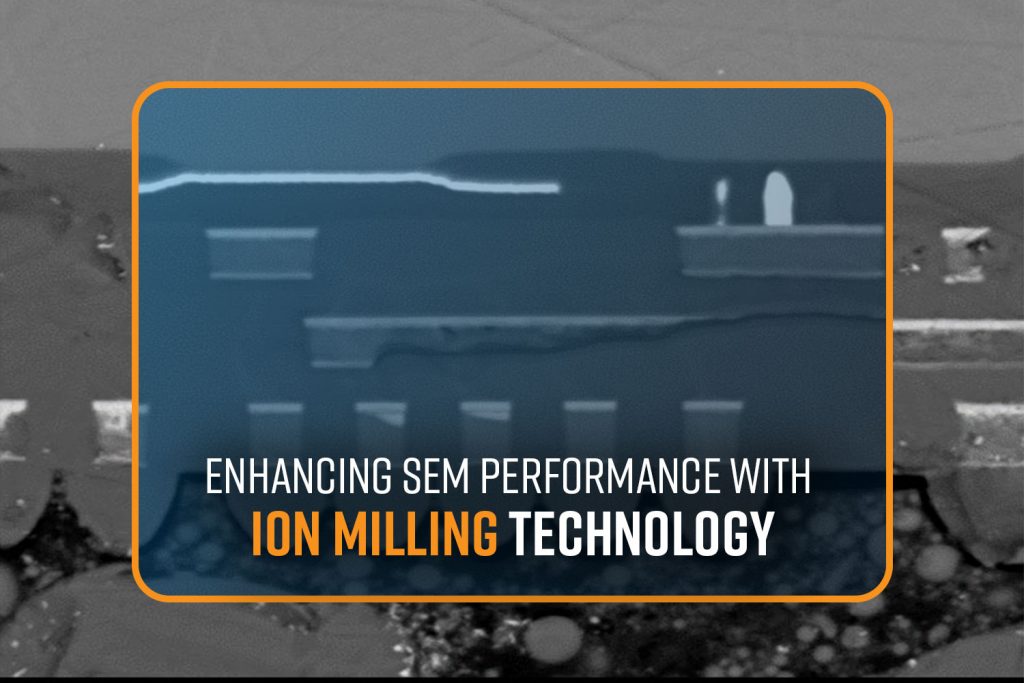
In material science, cross-section polishing is a critical method to enable the detailed examination of a sample material’s microstructure. This technique is essential for understanding the composition, properties, and potential applications of various materials, from metals and ceramics to semiconductors and battery materials. By providing a pristine, flat, and highly reflective surface, cross-section polishing enables researchers and engineers to see inside the microscopic world of materials with precision and clarity.
2-Day SEM Short Course | Alexandria, VA | September 2025

2-Day SEM Short Courses: Explore the microscopic world in our specialized 2-day Scanning Electron Microscopy (SEM) Short Course. Held in Alexandria, VA, this immersive program is designed for both experienced practitioners and newcomers, offering an in-depth exploration of both fundamental and advanced SEM techniques. Hosted at our state-of-the-art facilities, the course features hands-on sessions with […]
Benchtop STEM-in-SEM: A Powerful Tool for Tissue Ultrastructure Studies
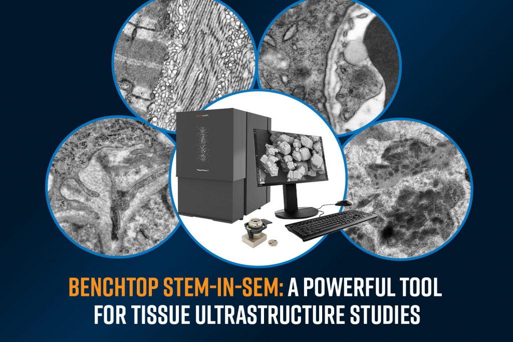
Understanding the ultrastructure of biological tissues is essential for advancing medical research, disease diagnostics, and drug development. Traditionally, histological techniques such as optical microscopy have been the standard for tissue analysis. While these methods provide valuable insights, they are often limited in resolution, making it difficult to visualize fine structural details at the nanometer scale. […]
Essentials of Polymer Compounding
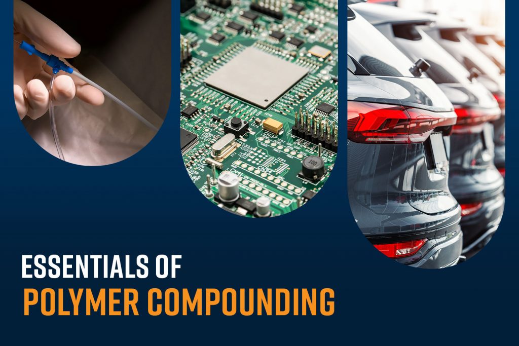
Polymer compounding is a fundamental process in materials engineering that involves blending polymers with various additives to enhance their properties and performance. This allows manufacturers to tailor polymer materials to meet specific requirements for different industries including automotive, aerospace, healthcare and consumer goods. By tailoring the mechanical, thermal, and chemical properties of polymers, their range of applications can be significantly increased.
Automated SEM: The Future of Particle Analysis
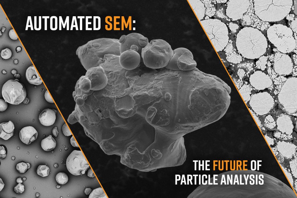
Particle analysis involves characterizing the size, morphology, and composition of powders and particulate matter to describe their properties in a precise and statistically significant manner. Some of the most common areas where particle analysis is critical are in advanced manufacturing, forensic analysis, and environmental applications. Among the different techniques for conducting particle analysis, scanning electron […]
2025 NanoNews: SEM Edition Q1
We’re pleased to share the latest edition of nanoNews! In the first quarter of the 2025 newsletter, you’ll find our webinar resources, event news, and our newest articles and technical notes – all focused on Scanning Electron Microscopy (SEM).
AISTech 2025 | May 5-7, 2024 | Nashville, TN

Association for Iron & Steel Technology Conference 2025 At Nanoscience Instruments, we empower steelmakers by equipping them with the means to achieve comprehensive inclusion analysis in one automated system: desktop scanning electron microscopy (SEM) combined with energy dispersive X-ray spectroscopy (EDS). Automated SEM-EDS forms the functional backbone of the Phenom ParticleX Steel system, elevating high […]
8 Factors That Affect the Cost of a Force Tensiometer
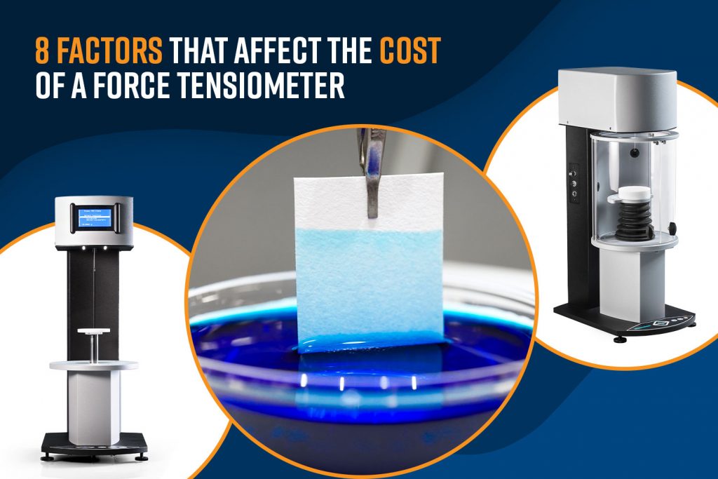
A force tensiometer is an instrument that uses a highly sensitive analytical balance and specialized probes to characterize several key interfacial properties. Even though it is most used to measure surface and interfacial tension, force tensiometers are capable of a variety of other measurements including contact angle, adhesion and cohesion, critical micelle concentration, and powder wettability.
5 Reasons to Use a Desktop STEM to Screen Negatively Stained Samples
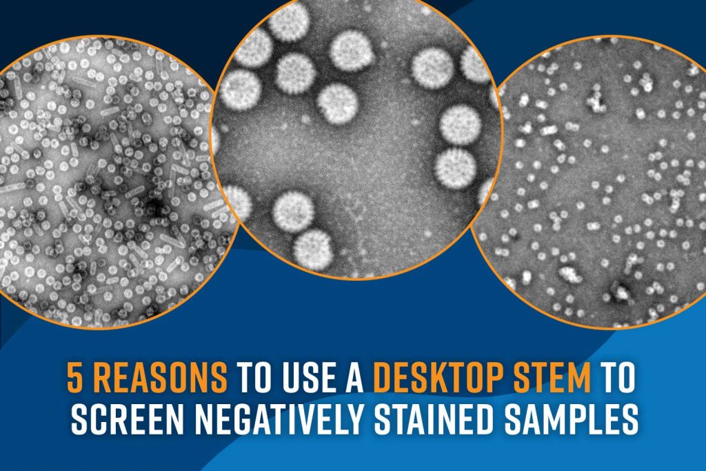
Cryo-electron microscopy (cryo-EM) is a powerful imaging technique used to determine the structure of biological macromolecules, viruses, and cellular components at near-atomic resolution. Unlike traditional electron microscopy, which requires heavy metal staining or dehydration, cryo-EM preserves biological samples in their native hydrated state by rapidly freezing them.
Advanced Automation Features of QSense Omni for Maximizing Efficiency
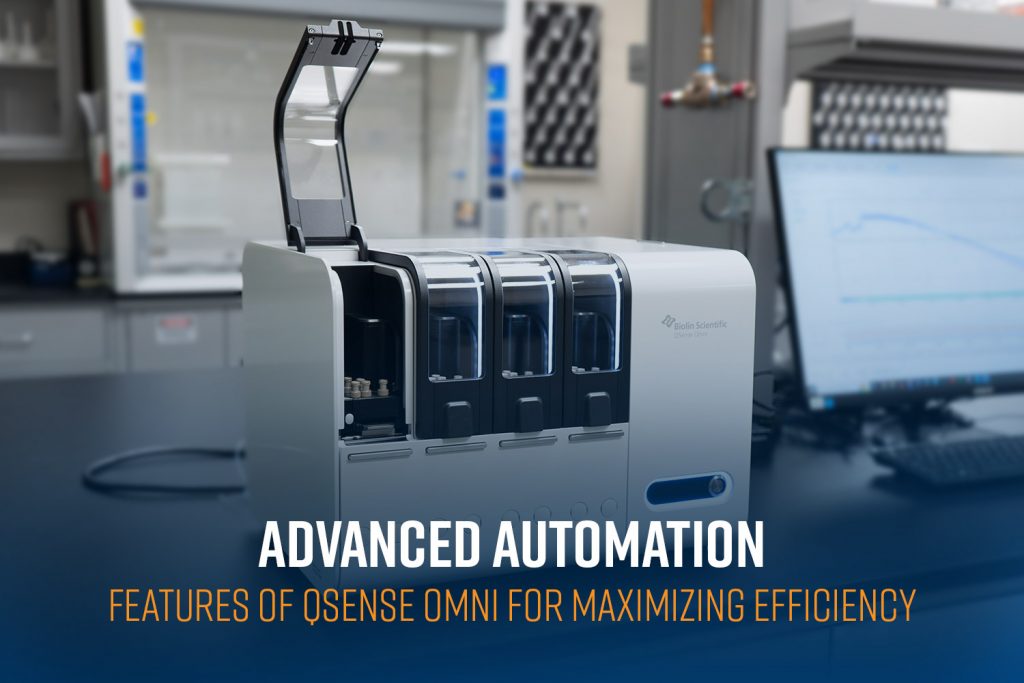
Quartz Crystal Microbalance with Dissipation monitoring (QCM-D) has revolutionized surface science by enabling real-time analysis of molecular interactions. However, traditional QCM-D workflows often involve time-consuming manual processes that introduce variability and inefficiency. In most QCM-D systems, sensor mounting, determining the resonance frequencies, stabilizing the baseline in air, priming the sensor, and establishing the baseline in liquids are performed manually.