Tech Note | Technology: Ion Milling, Scanning Electron Microscopy
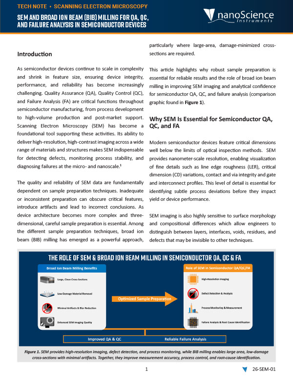
Introduction As semiconductor devices continue to scale in complexity and shrink in feature size, ensuring device integrity, performance, and reliability has become increasingly challenging. Quality Assurance (QA), Quality Control (QC),…
Tech Note | Technology: Electrospinning
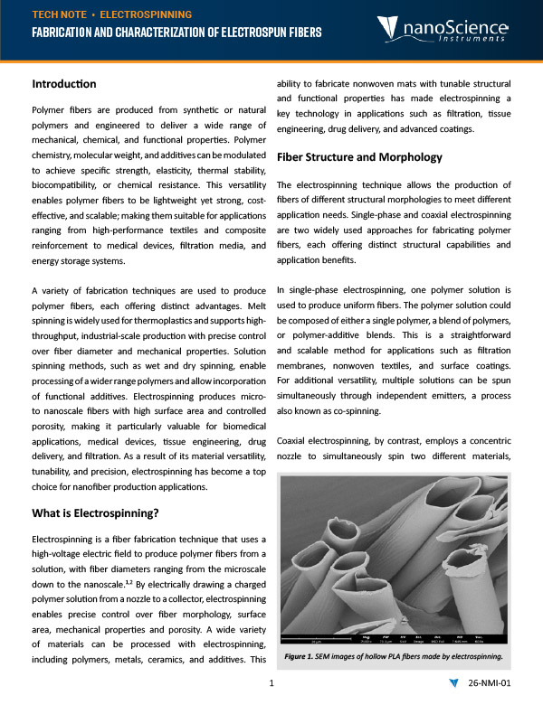
Polymer fibers are produced from synthetic or natural polymers and engineered to deliver a wide range of mechanical, chemical, and functional properties. Polymer chemistry, molecular weight, and additives can be…
Tech Note | Technology: Scanning Electron Microscopy
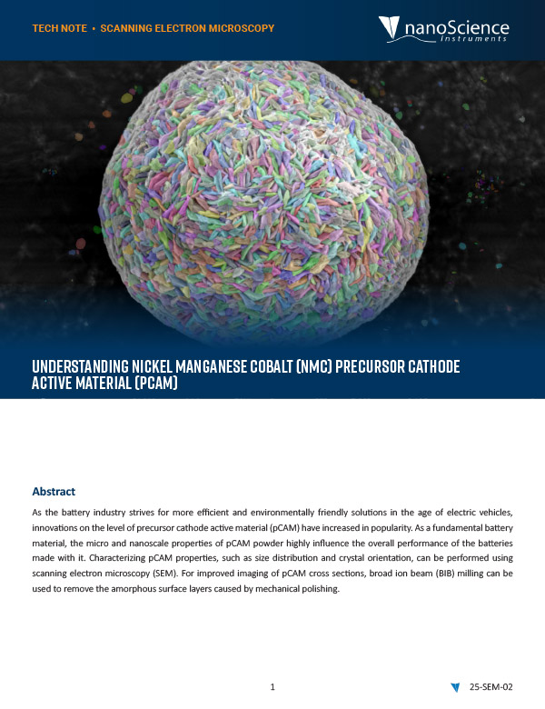
As the battery industry strives for more efficient and environmentally friendly solutions in the age of electric vehicles, innovations on the level of precursor cathode active material (pCAM) have increased…
App Note | Technology: Electrospinning
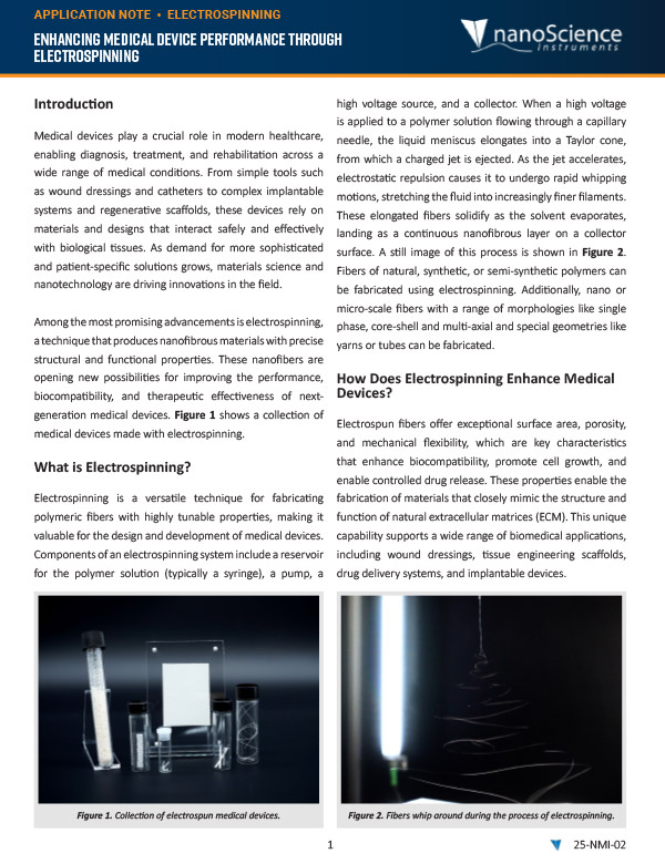
Medical devices play a crucial role in modern healthcare, enabling diagnosis, treatment, and rehabilitation across a wide range of medical conditions. From simple tools such as wound dressings and catheters…
App Note | Technology: Electrospinning
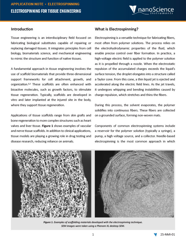
Advancements in the field of tissue engineering help improve medical treatment outcomes by accelerating healing, improving infection resistance, and reducing the need for human donors. By combining key principles from…

Tech Note | Technology: Scanning Electron Microscopy
In today’s precision-driven manufacturing landscape, part cleanliness isn’t just a quality benchmark, it’s a critical factor that can make or break product performance and reliability. This is especially relevant in…
Tech Note | Technology: Force Tensiometry, Optical Tensiometry
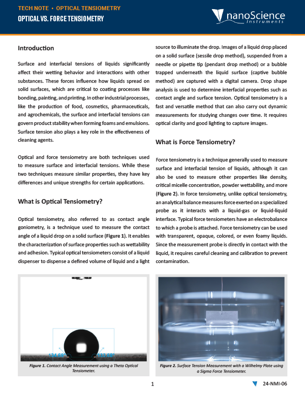
Surface and interfacial tensions of liquids significantly affect their wetting behavior and interactions with other substances. These forces influence how liquids spread on solid surfaces, which are critical to coating…
Tech Note | Technology: Scanning Electron Microscopy
The Phenom Pharos Desktop SEM/STEM is a compact and affordable solution designed for cryo-electron microscopy groups and core facilities looking to streamline experimental workflows. This technical note evaluates the Phenom…
Tech Note | Technology: Optical Tensiometry
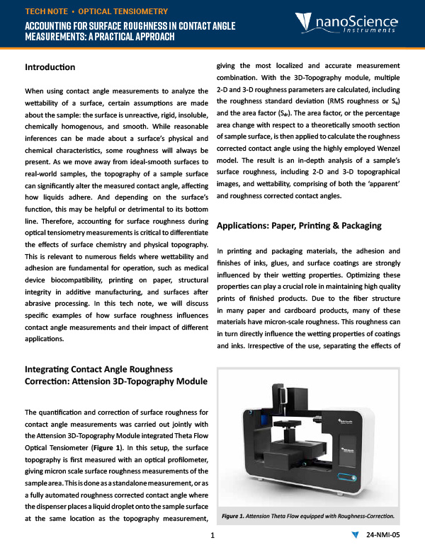
Contact angle measurements are a fundamental tool to understand the chemistry of surfaces and their wetting properties. Typically measured with side-on optical tensiometry, contact angle measurements are carried out by…
Tech Note | Technology: Scanning Electron Microscopy
In modern steel manufacturing, non-metallic inclusions represent a critical quality concern due to their effects on mechanical properties and overall steel functionality. Scanning electron microscopy (SEM) and energy dispersive X-ray…
This site is protected by reCAPTCHA and the Google Privacy Policy and Terms of Service apply.