
Microscopy & Microanalysis 2024 | July 29 – August 1, 2024 | Cleveland, Ohio

Join us in Cleveland, Ohio for the highlight of the microscopy calendar – M&M 2024! Nanoscience Instruments is back for this annual summertime conference, and this time we’re showcasing in Booth #527.
Advancing Wound Care with Electrospinning
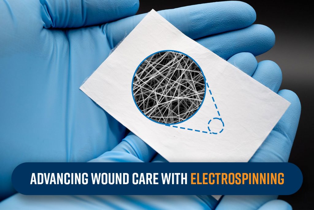
Wound care solutions are essential in medicine to protect injuries from infection, manage exudate, and create an optimal healing environment. Effective solutions promote faster and more efficient healing, reducing the risk of complications and scarring. There is a continuous quest for innovative wound care solutions to improve patient outcomes and overall quality of life by supporting tissue regeneration and providing pain relief. Electrospinning is an advanced technology that has demonstrated the potential to transform wound care through its ability to create nanofibrous scaffolds with tailored properties. In this blog, we’ll delve into the applications of electrospinning in wound healing and explore how this technique is helping shape the future of healthcare.
Struck by an Electron Beam: Interactions at the Surface in SEM
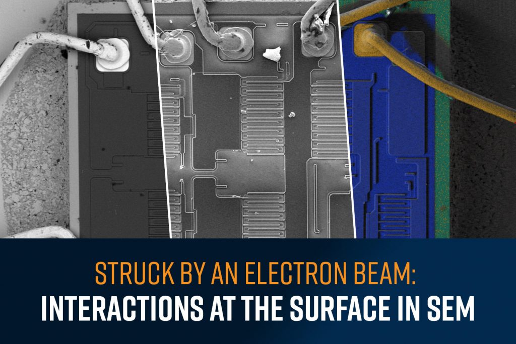
Scanning Electron Microscopy (SEM) is one of the most important tools in the arsenal of modern material science used to characterize micro and nanoscale features. Central to its functionality is the interaction between a finely focused electron beam and the sample. As these electrons meet the surface, they elicit various responses: backscattering, secondary electron emission, X-ray generation, and cathodoluminescence, each carrying unique information about the sample’s composition and structure (Fig 1). These signals can be processed to visualize and better understand the materials [1]. This blog examines these interactions, describes how they occur, the types of signals they produce, and the implications of these signals for material analysis.
Improving Microstructural Analysis in SEM Imaging with Gamma Correction

A scanning electron microscope (SEM) is capable of visualizing compositional heterogeneity on the surface of a sample by employing a backscattered electron detector (BSD). A BSD works by detecting elastically scattered electrons that are reflected from the sample surface as the electron beam is scanned across its surface. The higher the atomic number of the material, the more backscattered electrons will be generated, resulting in higher contrast in the BSD image. This mode of imaging in SEM provides valuable insights regarding the microstructure of the material under study.
SEM Imaging of Uncoated, Nonconductive Samples
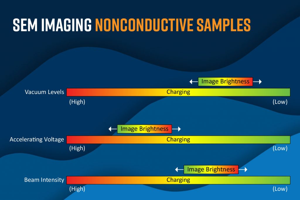
Scanning Electron Microscopy (SEM) generates high-resolution images by scanning a focused beam of electrons across the sample surface and detecting the signals produced through beam-sample interactions. Imaging nonconductive samples by SEM poses a challenge since they accumulate electrostatic charge at their surface during imaging, resulting in a variety of imaging artifacts. Therefore, mitigating the effects of charge accumulation is essential for ensuring reliable SEM analysis of non-conducting materials.
The Electrochemical Society 2024 | May 27-29, 2024 | San Francisco, CA

245th Electrochemical Society Meeting Nanoscience Instruments combines expertise in scientific instrumentation with real-world solutions, providing not only the tools to accelerate electrochemical research and development, but also expert application support, field service, and analytical testing. Our suite of solutions for electrochemists includes several cutting-edge tools that support advanced material development and characterization, such as: Our […]
AISTech 2024 | May 6-8, 2024 | Columbus, Ohio

Association for Iron & Steel Technology Conference 2024 At Nanoscience Instruments, we empower steelmakers by equipping them with the means to achieve comprehensive inclusion analysis in one automated system: desktop scanning electron microscopy (SEM) combined with energy dispersive X-ray spectroscopy (EDS). Automated SEM-EDS forms the functional backbone of the Phenom ParticleX Steel system, elevating high […]
Gold vs Platinum: Choosing the Right Coating for SEM Imaging

One of the most common challenges when analyzing non-conductive samples with a scanning electron microscope (SEM) is the charging effect. Without a conductive path, the electrons accumulate at the surface, resulting in a distorted image with skewed grayscale values. Although, in some cases, adjusting electron beam parameters and imaging conditions can be sufficient for mitigating charge build-up, sputter coating a conductive layer remains the most effective method for reducing sample charging. Gold and platinum are the most common metals used for sputter coating SEM samples.
Infrastructure Essentials: Preparing Your Workspace for a Phenom Desktop SEM

Integrating the ability to perform high-resolution imaging and compositional analysis of materials into any laboratory becomes simplified with a desktop scanning electron microscope (SEM). In addition to the compact footprint, desktop (synonymously benchtop or tabletop) SEMs are engineered for speed, reliability, and ease of use. Consequently, numerous organizations are contemplating acquiring desktop SEMs as an in-house solution to enhance their competitiveness in manufacturing or research and development capabilities.
Cutting Costs, Not Corners: Why Phenom Desktop SEMs are a Smart Investment

When acquiring a new scanning electron microscope (SEM), it can be challenging to identify a solution that not only delivers exceptional performance but also remains financially feasible. Among the myriad of options available, Phenom Desktop SEMs have emerged as a leader in affordability without compromising on quality or functionality. Widely regarded as the best-selling desktop SEMs on the market, Phenom SEMs embody the capabilities of larger, floor-model SEMs without the barrier of a complex user interface.