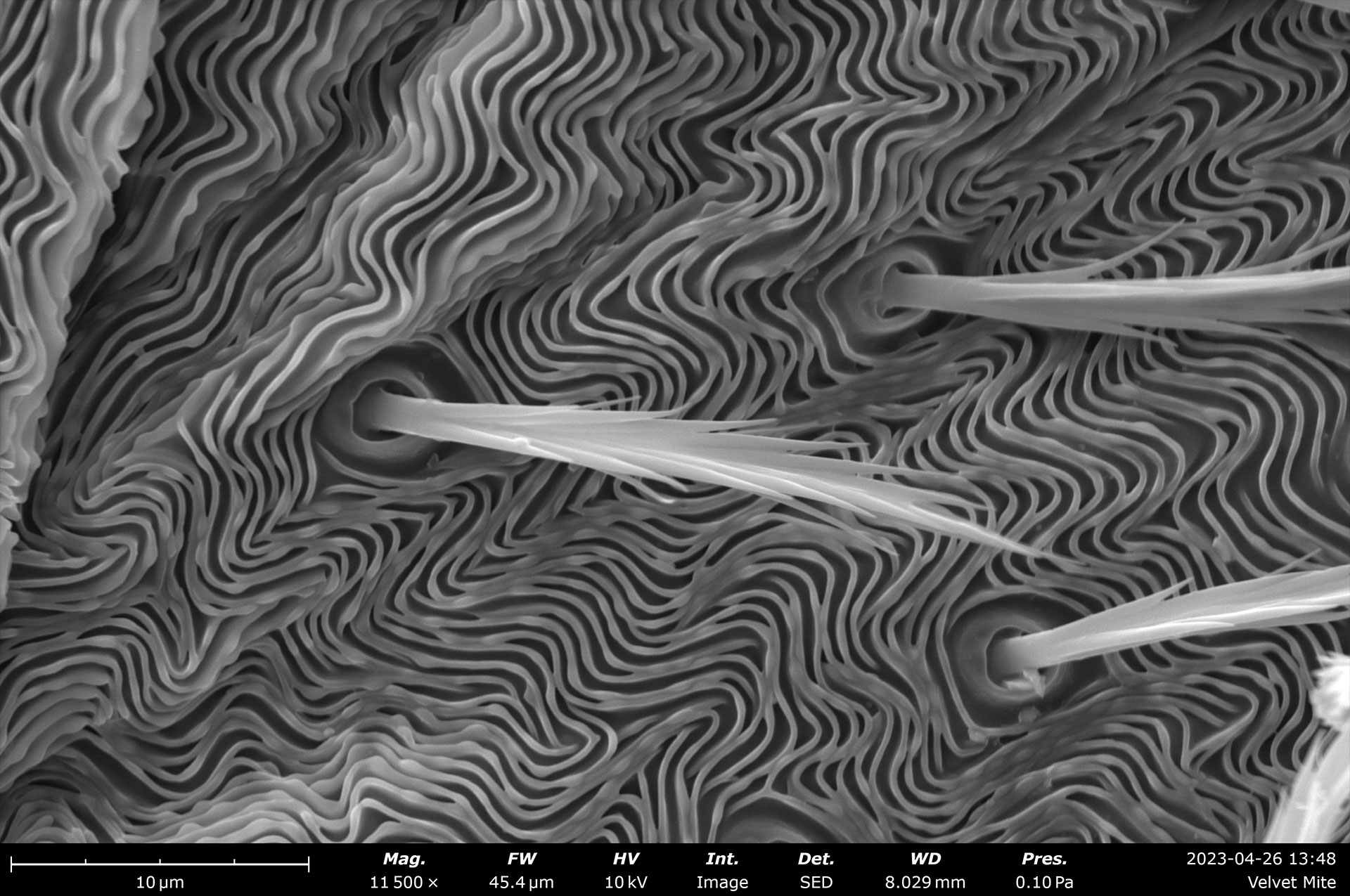
What is Scanning Electron Microscopy?
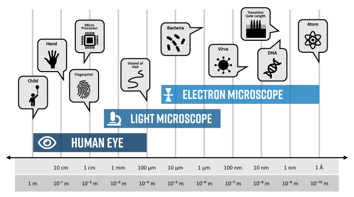
Scanning electron microscopy is a highly versatile technique used to obtain high-resolution images and detailed surface information of samples. It is a type of electron microscopy that uses a focused beam of electrons to scan the surface of a specimen and generate images at a much greater resolution compared to optical microscopy. The resolution of SEM instruments can range from < 1 nanometer up to several nanometers.
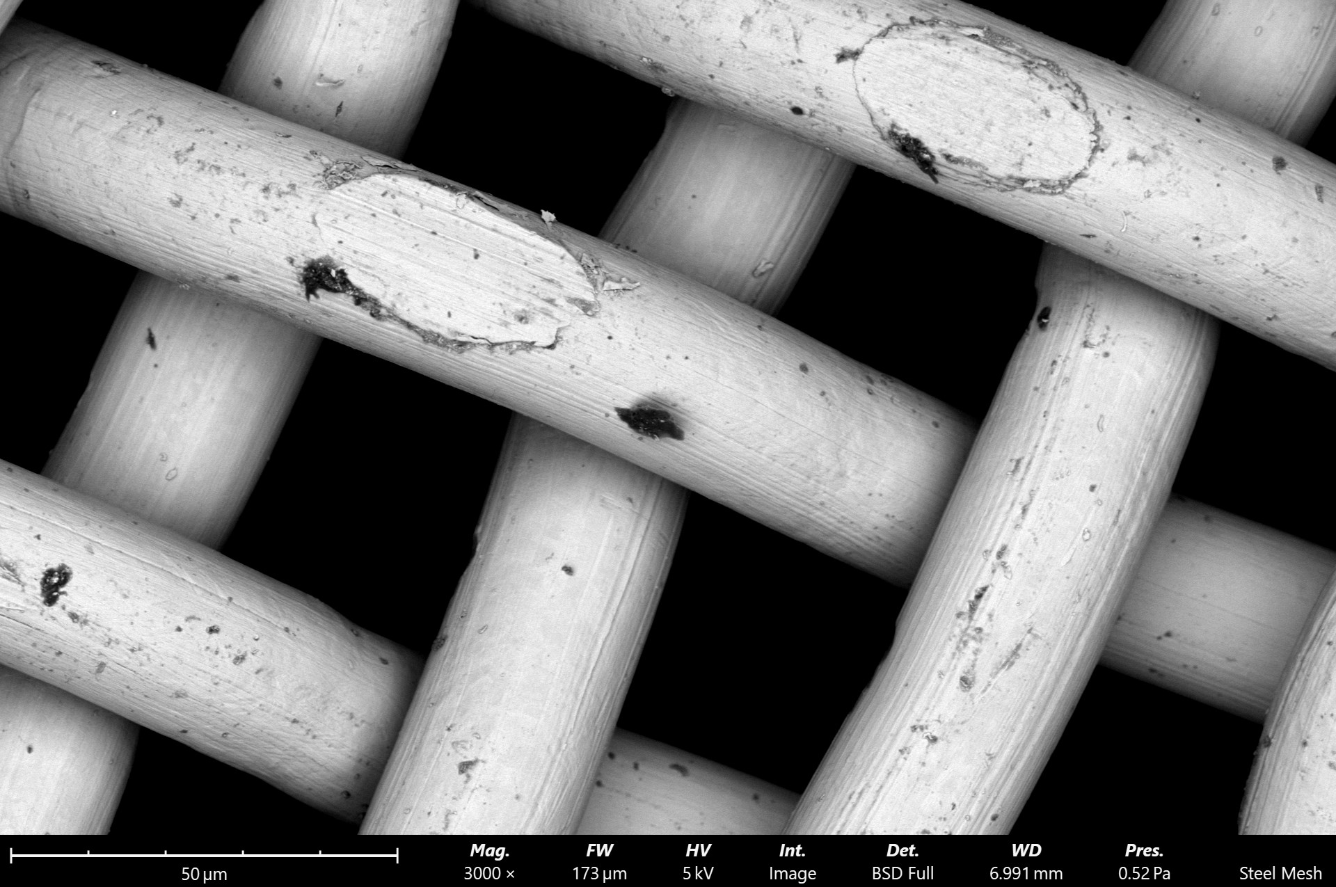
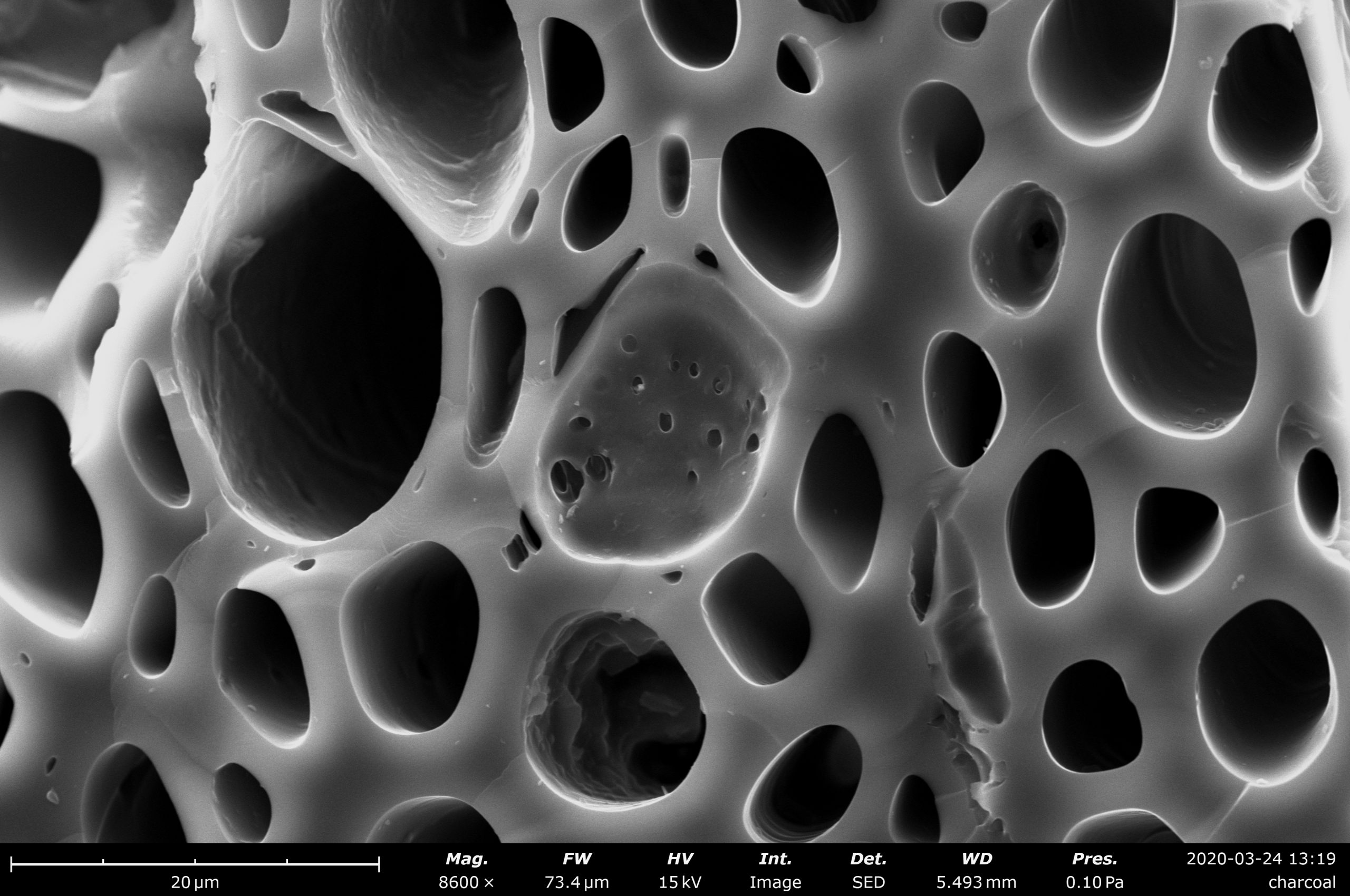
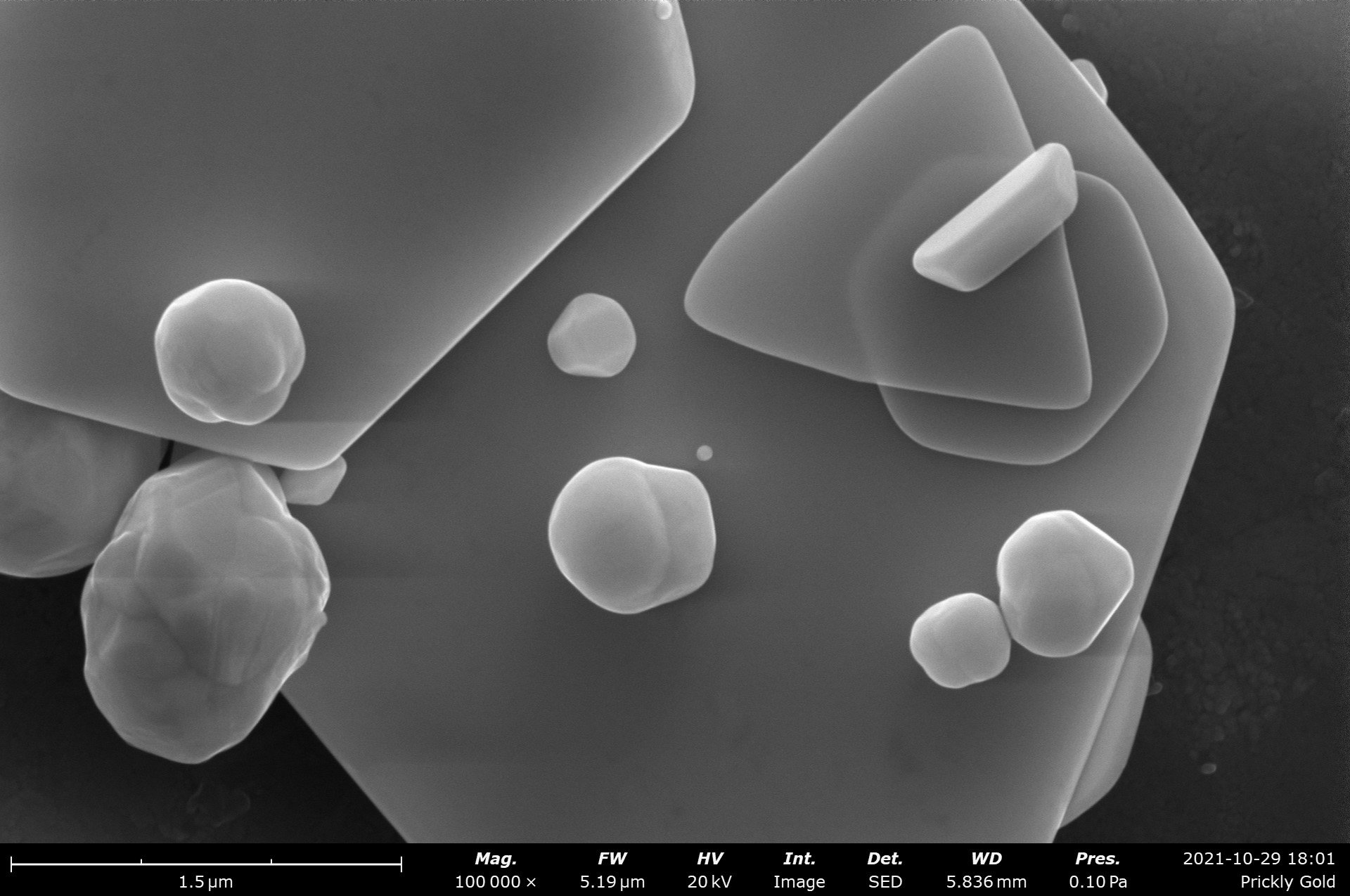
A scanning electron microscope (SEM) projects and scans a focused stream of electrons over the surface of a sample and collects the different signals produced using specialized detectors. The electrons in the beam interact with the atoms within the sample, thereby producing various signals that can be used to obtain information about the surface’s topography and composition. Images are viewed in real-time on an external monitor using software that correlates the beam’s position with the intensity of electrons acquired by the detector(s). A secondary electron detector (SED) and a backscattered electron detector (BSD) are the two most common types of detectors used for high-resolution imaging in an SEM. Microanalysis of the surface composition can be accessed using energy dispersive X-ray spectroscopy (EDS) detectors. The unique configuration of the SEM will ultimately determine its resolution and available imaging modes.
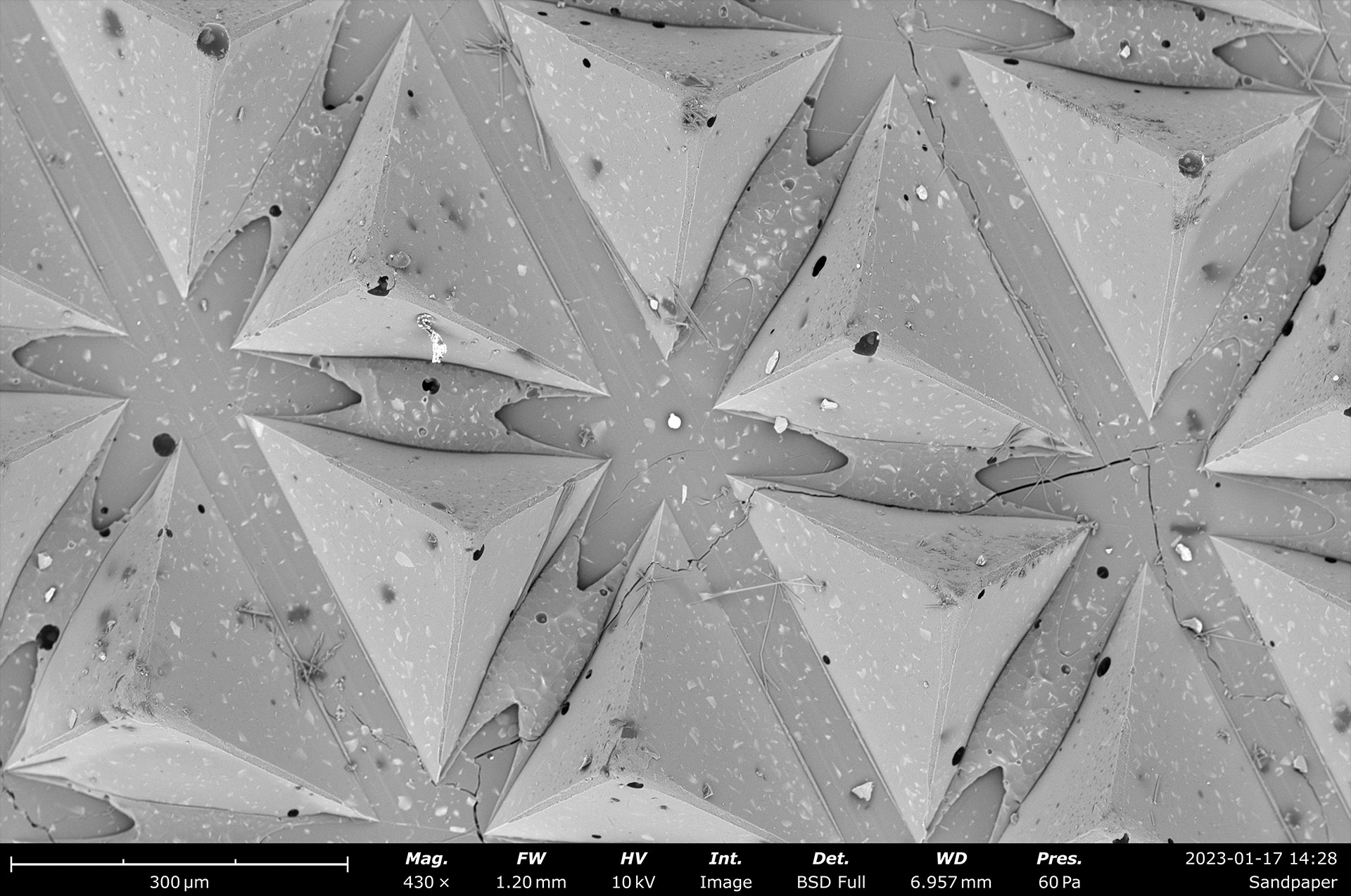
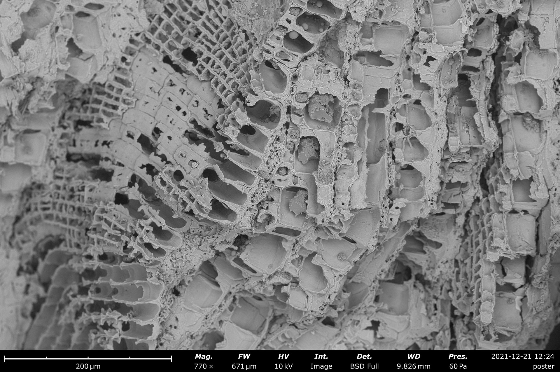
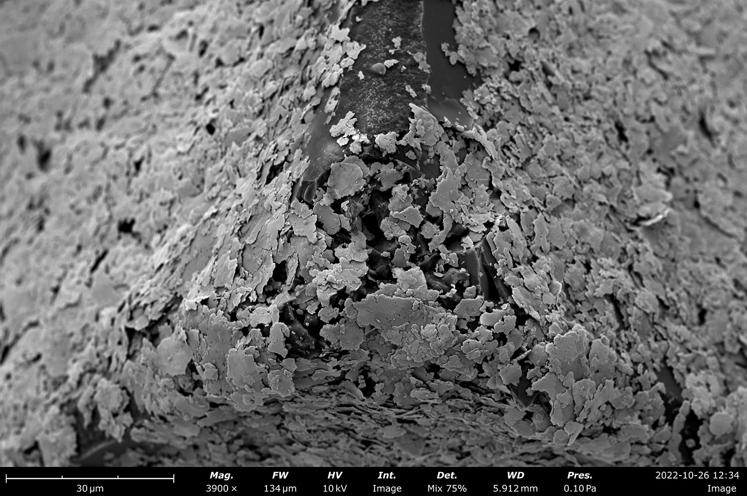
A wide range of solid materials can be directly analyzed using SEM. Biological materials and insulating samples often require specialized imaging, such as low-vacuum or low-kV imaging, to reduce surface charging and beam damage. Insulating samples can be sputter coated with a thin layer of gold or platinum to minimize charging.
Why use electrons instead of light in a microscope?
Light Microscope theoretical resolution:
δ |
= |
0.61 λ |
||
μ sinβ |
||||
δ = smallest resolvable distance (i.e., resolution) | λ = incident wavelength | μ = refractive index of viewing medium | β = semi-angle of microscope’s aperture
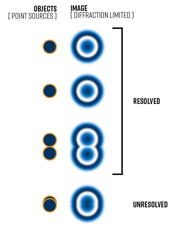
The equation assumes the imaging process is diffraction-limited, meaning other factors like imperfect lenses or optical misalignments are not influencing resolution. In other words, this is the theoretical limit of resolution. Simplifying μ sinβ (i.e., the numerical aperture) to one sets a general rule for light microscope resolution as about half the incident light wavelength.
Wavelength of Fast electron:
λ |
= |
h |
||
√2meV |
||||
h = Planck’s constant (6.626 x 10⁻³⁴ m2kg/s) | m = mass of electron (9.109 x 10⁻³¹ kg) | e = electron charge (1.60 x 10⁻¹⁹ C) | V = accelerating voltage
| Accelerating Voltage | Type of Electron Microscope | Electron Wavelength, λ |
| 5 kV | SEM | 0.0172 nm |
| 10 kV | 0.0122 nm | |
| 20 kV | 0.0086 nm | |
| 200 kV | TEM/STEM | 0.0027 nm |
SEM accelerating voltages range from less than 5 keV up to 30 keV. The most powerful electron microscopes, namely the transmission electron microscope (TEM) and scanning transmission electron microscope (STEM) can reach up to 300 keV or higher. This vast difference between the wavelength of accelerated electrons and that of visible light is what gives electron microscopes the potential for undertaking the task of visualizing materials on atomic and nanometer length scales. In practice, the diffraction-limited resolution is not actually achieved because of imperfect electromagnetic lenses. Nonetheless, electron microscopes like SEMs offer tremendous resolution improvements over light microscopes.
Optical Microscope vs. a Scanning Electron Microscope
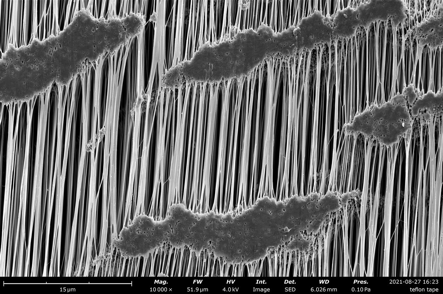
Optical (light) microscope lacks resolution and depth of field when compared to the SEM. The depth of field is an important concept in microscopy that defines the portion of the image that is reasonably in focus.2 In the example below, a nanofiber layer used for filtration is imaged over the same area using an optical microscope and an SEM. In the optical image, many of the fibers appear blurry and out-of-focus owing to the poor depth of field inherent to light microscopy. It also means that multiple images would need to be acquired at different focal lengths to obtain a complete view of the specimen. On the other hand, the entire region is crisply in focus when analyzed in the SEM. The contrast is also much improved in the SEM, allowing for more accurate detection and potential measurements of fiber dimensions.


A) Optical microscope image of nanofibers.
B) Scanning electron microscope image at 4000x magnification of the same nanofibers.

How a Scanning Electron Microscope Works
Electrons are produced at the top of the column in the electron gun and accelerated through the column at a specified accelerating voltage (1 keV – 30 keV). Condenser lenses and apertures act to reduce the beam diameter. The final lens in the column is the objective lens, which focuses the beam on the sample surface. The diameter of the beam in an SEM can range from <1 nanometer up to 20 nanometers, depending on the type of electron gun, accelerating voltage, and lens configuration. The sample itself is mounted on a stage in the chamber area and both the column and the chamber are maintained under vacuum by a combination of pumps. The level of the vacuum will depend on the design of the microscope. Some microscopes allow for variable pumping, allowing the sample chamber to be kept at a lower vacuum level than the rest of the column in order to support low-vacuum imaging.
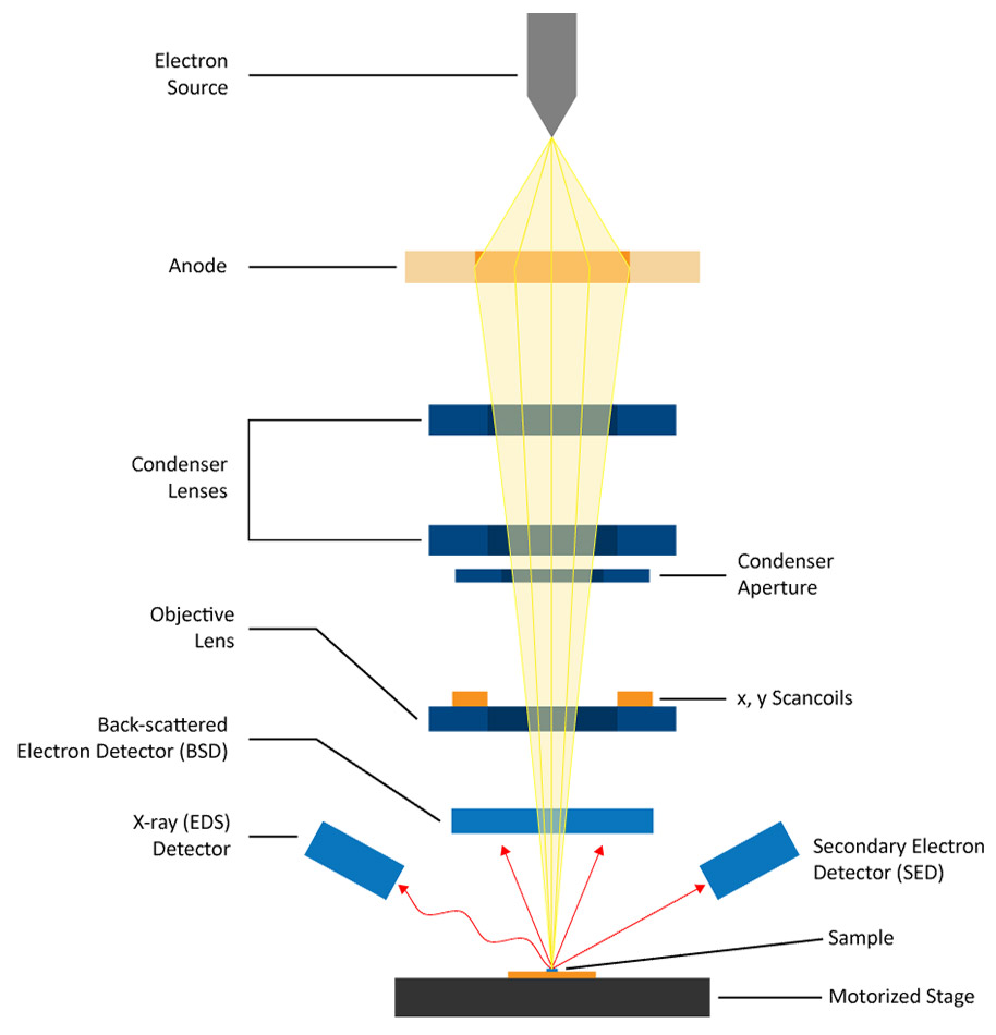
The position of the electron beam on the sample is controlled by scan coils situated above the objective lens. These coils allow the beam to be scanned over the surface of the sample in the X-Y plane. The scanned beam strikes the sample, generating a variety of signals including secondary electrons, backscattered electrons, and characteristic X-rays. These signals are then detected by appropriate detectors.
The scan generator, together with an external computer containing specialized software, is able to sync the information from the scan generator (containing the beam’s X,Y position at each period in time) with the intensity acquired by the detector, allowing a grayscale image to be displayed and viewed in real time pixel-by-pixel. Depending on the dwell time of the electron beam at each X,Y position, the signal-to-noise can be modulated. Magnification results from the size of the scanned area, wherein higher magnifications correspond to progressively smaller scanned areas. The number of pixels may also be adjusted within a given scan area, which can impact the apparent resolution.
Sample-Electron Interactions
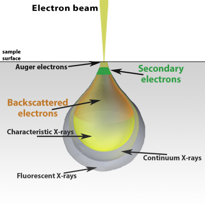
Many signals are generated as a result of the electron beam interacting with the sample. The most used signals in the SEM are secondary electrons, backscattered electrons, and characteristic X-rays. Certain materials may emit photons when excited by the electron beam through a process known as cathodoluminescence.
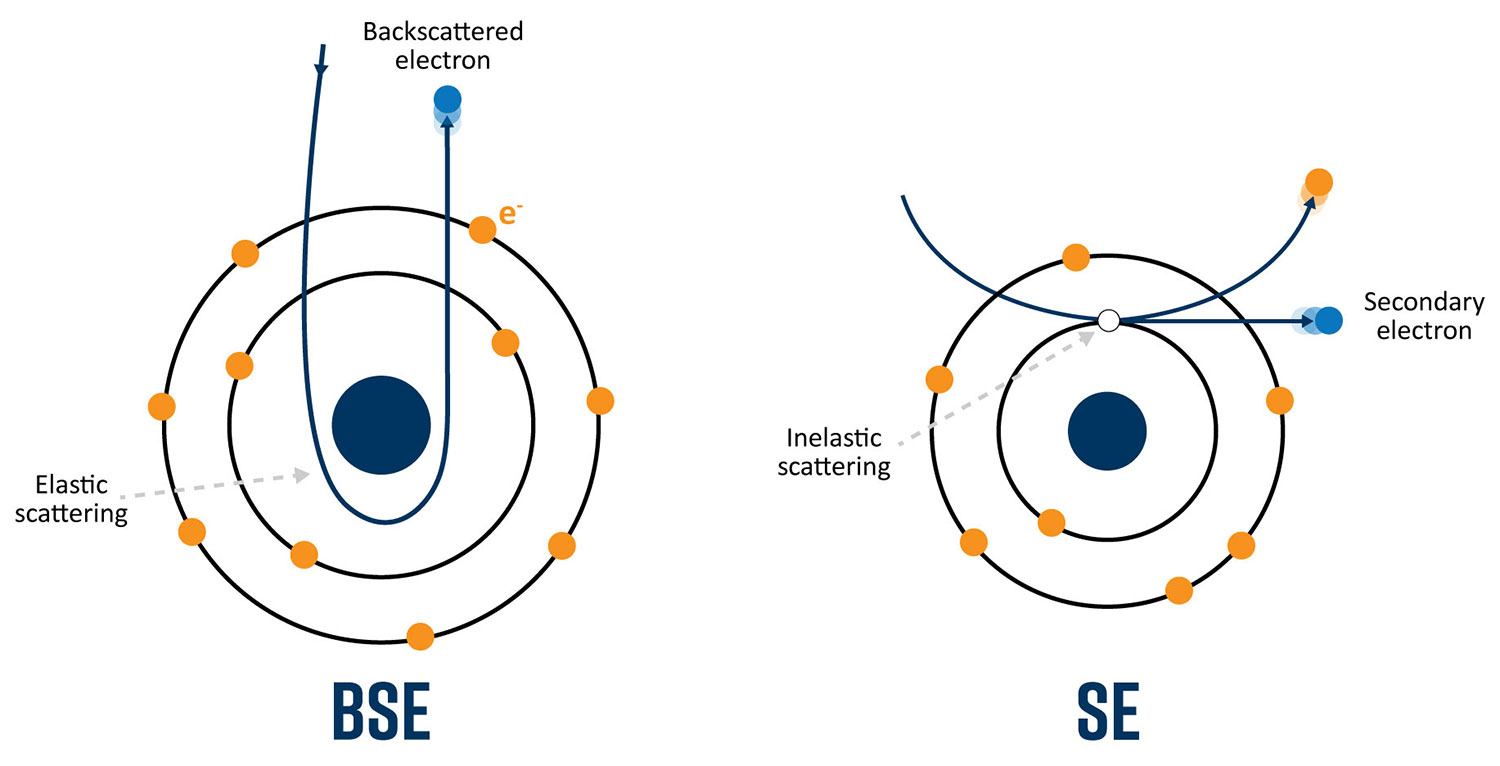
Secondary electrons are primarily used for topographical images because they are generated closer to the surface of the sample. A secondary electron is emitted because of inelastic scattering, or interactions that involve energy transfer from a primary beam electron to an atom in the sample. The energy of secondary electrons is defined as being less than 50 eV. Images collected with secondary electrons will also possess the best lateral resolution due to the relatively small interaction volume that is approximately the size of the beam diameter.
Elastic scattering at high angles (> 90°) results in the emission of backscattered electrons above the surface of the sample. When the primary beam approaches the nucleus of an atom in the sample, the positive charge causes a deflection of the fast electron causing it to be remitted from the surface. The yield of backscattered electrons depends upon the average atomic number wherein heavier elements, possessing more positive charge, result in higher yield. Therefore, the contrast in images acquired with backscattered electrons provides information on surface composition.
Characteristic X-rays are emitted when an ionized atom relaxes to a ground state by filling an inner shell electron hole with an electron from a higher orbital. The energy difference between the two electron shells is equivalent to the characteristic X-ray energy and can be used to fingerprint the specific element that it originated from. Compared to backscattered electrons, characteristic X-rays that result from inelastic scattering allow for precise identification of elements present in the sample. In addition to the characteristic X-ray peaks that are observed in EDS data, a continuum (background) signal is generated by the deceleration of incident electrons as they interact with the sample.
The maximum resolution obtained in an SEM depends on multiple factors including the electron beam spot size and interaction volume of the electron beam with the sample. While it cannot provide atomic resolution, some SEMs can achieve resolution below 1 nm.
Components in a SEM
The main SEM components include:
- Electron source (gun)
- Condenser lenses
- Objective lens
- X-Y scan coils & scan generator
- Detectors
- Sample stage
- Computer and display to view the images
- External vacuum pump(s)
Electron Source
The electron source is a crucial element of a scanning electron microscope (SEM) because it significantly influences its analytical performance. Commonly referred to as the electron gun, this component needs to emit a bright and coherent stream of electrons that can be defocused onto the sample by lenses within the column. SEMs typically utilize three prevalent types of electron emitters: tungsten filaments, solid-state hexaboride crystals, and field emission guns.
Tungsten (W) Filament
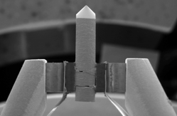
This consists of an inverted V-shaped wire of tungsten, about 100 µm long, which is heated resistively to produce electrons. This is the most basic type of electron source and was developed for the first generation of electron microscopes. It remains the most common type of electron source to this day because it is low-cost. The emission area of a tungsten hairpin is relatively large, meaning that the resolution is supplies is also the lowest. Since they operate at extremely high temperatures (~2800 K), the tungsten gradually evaporates over time leading to contamination of the column. This also renders tungsten filaments susceptible to abrupt burnout after about 100 hours of beam-on operation. SEM instruments containing tungsten sources also require frequent adjustment of beam stigmation and alignment because they are sensitive to thermal fluctuations.
Lanthanum Hexaboride (LaB6) or Cerium Hexaboride (CeB6)
Field Emission Gun (FEG)
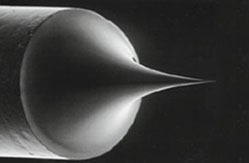
The FEG source is a wire of tungsten with a very sharp tip, less than 100 nm, that uses field electron emission to produce the electron beam. The process works through electron tunneling wherein an electric field is applied to the tip to extract the electrons, and a second field is used to accelerate them down the column. Schottky FEGs are typically used in SEM. These sources function as field-assisted thermionic emitters. FEG sources produce electron beams with the highest brightness and coherence, allowing the highest resolutions to be obtained.
Comparison of electron source characteristics for SEM
| Tungsten hairpin | CeB6 crystal | Schottky FEG | |
| Emission mechanism | Thermionic | Thermionic | Electron Tunnelling |
| Lifetime | 100 h | 1500 h | >10,000 h |
| Tip emitting diameter | 100 µm | 25 µm | 100 nm |
| Resolution @30 kV | 4 nm | 3 nm | 1 nm |
| Resolution @1 kV | 50 nm | 25 nm | 5 nm |
| Low-kV imaging (<5 kV) | Yes | No | Yes |
| Vacuum | 10-1 – 10-5 mbar | 10-7 mbar | 10-9 mbar |
| Cost of ownership | Lowest | Medium | Highest |
Lenses
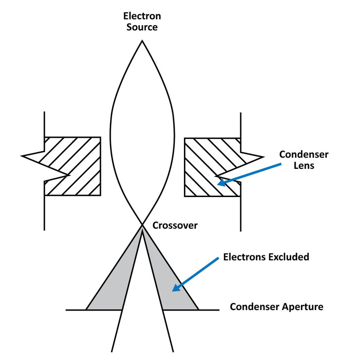
Electromagnetic lenses are used to manipulate the electron beam in an SEM. The lens is constructed of a solenoid of copper wire. Depending on the strength of the current passed through the solenoid, the applied magnetic field strength changes. As electrons pass through this magnetic field, off-axis electrons are bent toward the optic axis which causes a beam crossover to form at a specified distance from the lens.
The main purpose of a condenser lens is to reduce the diameter of the primary beam that is emitted from the electron source. A series of condenser lenses focus the electron beam as it moves from the source down the column. A condenser aperture may also be used to exclude off-axis electrons and further reduce the beam diameter. The narrower the beam the smaller the spot it will have when contacting the surface, thus the term ‘spot size’.
The objective lens is always the final lens in the column and focuses the beam onto the sample surface thereby establishing the working distance and probe size. Fine tuning the objective lens and objective aperture is important for optimizing the spatial resolution. Because of the differences in beam convergence angle (α), longer working distances (small α) correspond to a larger depth of field and lower spatial resolution compared to shorter working distances (large α).
Scanning Coil
After the beam is focused, scanning coils are used to deflect the beam in the X and Y axes so that it scans in a raster fashion over the surface of the sample. The scanning coils are synced with software that controls the detectors and the display of the image on an external monitor allowing real-time images to be viewed.
Sample Chamber
Samples are mounted and placed into a chamber that is evacuated. The sample chamber can include a translation stage, tilt and rotation devices, electrical feed-throughs to external devices, temperature-control stages for cryogenic cooling or heating, optical cameras, and a variety of other devices to assist in analyzing the sample.
Detectors
When the electron beam interacts with a sample in a scanning electron microscope (SEM), multiple events happen. In general, different detectors are needed to distinguish secondary electrons, backscattered electrons, or characteristic X-rays. Depending upon the accelerating voltage and sample density, the signals come from different penetration depths.
Backscattered electron detector (BSD)
A backscattered electron detector (BSD) detects elastically scattered electrons. These electrons are higher in energy and originate from below the surface of the sample. Therefore, the resolution of a BSD image will be worse than compared to an image acquired with an SED. Using a BSD allows for lower vacuum levels, reducing sample preparation requirements and minimizing beam damage.
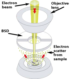
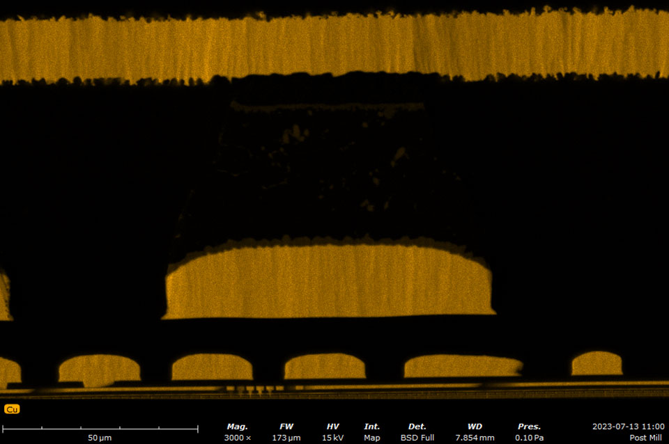
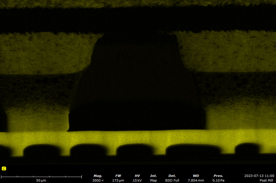
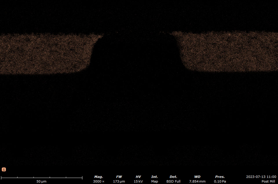
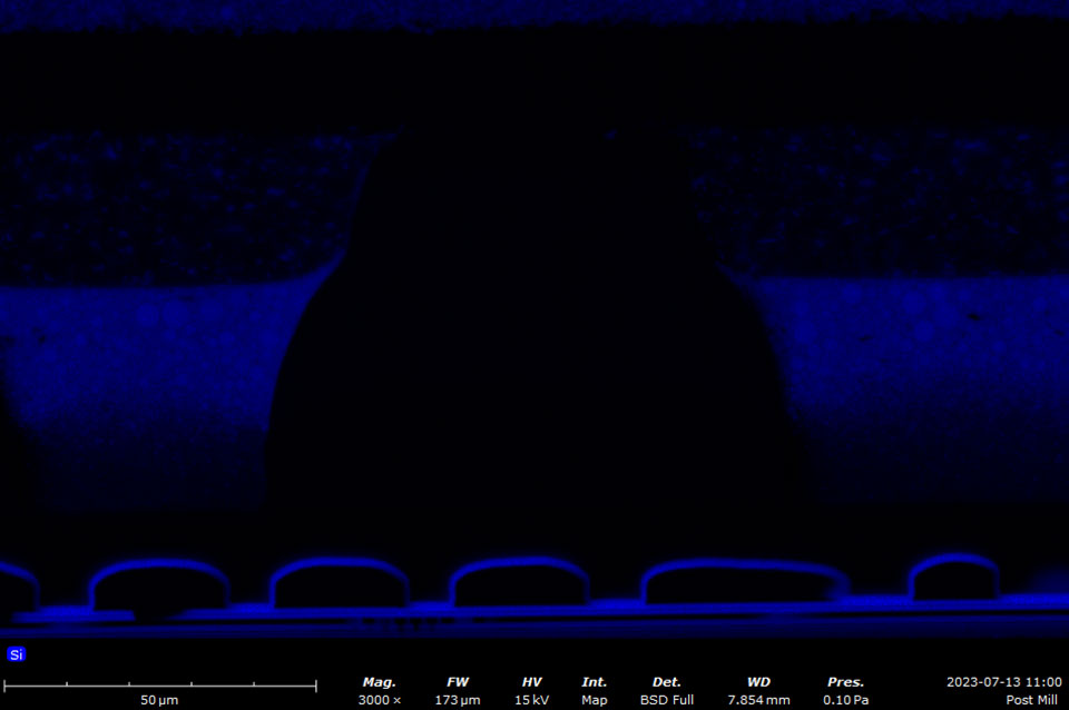
Backscattered electrons vary in their amount and direction due to the composition and topography of the specimen. The contrast of the backscattered electron image depends on multiple factors, including the atomic number (Z) of the sample material, the acceleration voltage of the primary beam, and the specimen angle (tilt) in relation to the primary beam. Materials with elements composed of higher Z elements yield more backscattered electrons than lower Z elements. BSD images can be used to quickly identify phases with different compositions.
The most common type of BSD is composed of a solid-state sensor. Incident electrons form electron-hole pairs in the semiconductor sensor material, generating a current that is proportional to the backscatter electron yield. A four-quadrant BSD is configured in an annulus around the optic axis above the sample. This design allows a large number of the backscatter electrons to be captured as well as providing individual signals in each quadrant, allowing for elemental contrast (composition) imaging and topographic imaging modes.
By adding the signal from all quadrants, the conventional BSD images can be generated that exhibit compositional contrast. Operating the BSD quadrants in pairs and then subtracting the signals yields topographic images. Compositional and topographic images can be acquired in the same location to provide insight to correlate material properties to topography, grain size, or morphology.
Secondary Electron Detector (SED)
A secondary electron detector (SED) for scanning electron microscopy offers images with resolution independent of the material. SED images allow for a visualization of the inelastically scattered electrons generated close to the sample surface and provide topographical information with the best possible resolution. No material composition information is available from SED images.
Secondary electrons are detected with an Everhart-Thornley (E-T) detector. The ET detector is composed of a scintillator inside a Faraday cage and is placed above the sample to one side. A positive bias is applied to the Faraday cage to attract the low-energy electrons where a scintillator converts the electrons into light (photons). The photon signals is then amplified using a photomultiplier tube to yield the final signal.
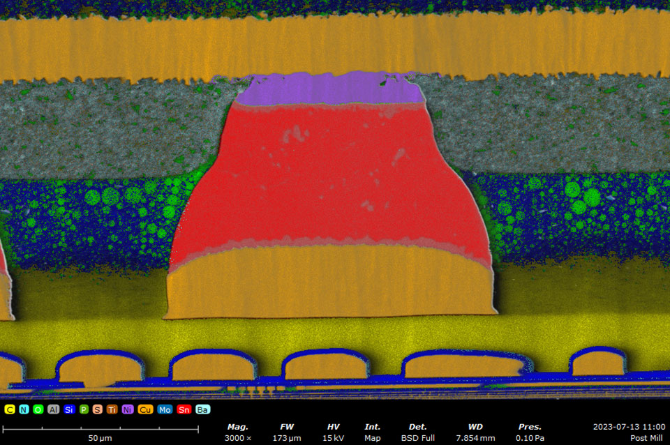
Energy Dispersive Spectroscopy (EDS)
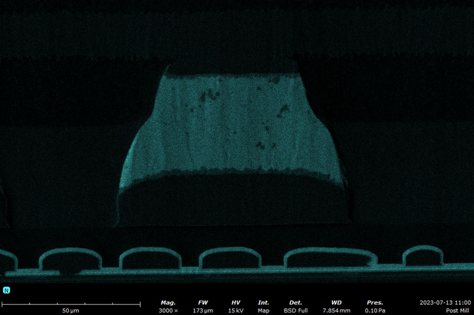
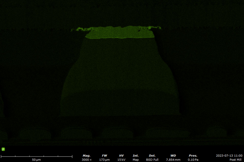
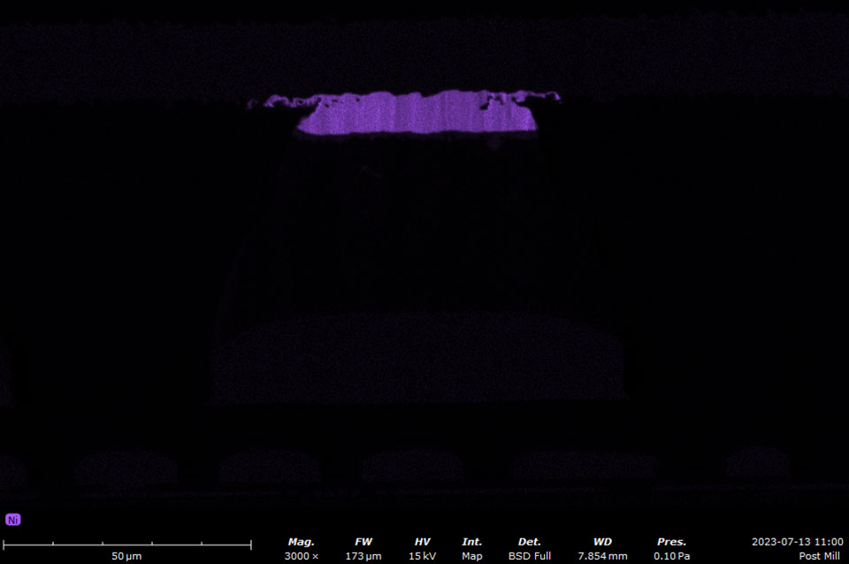
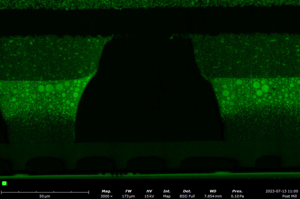
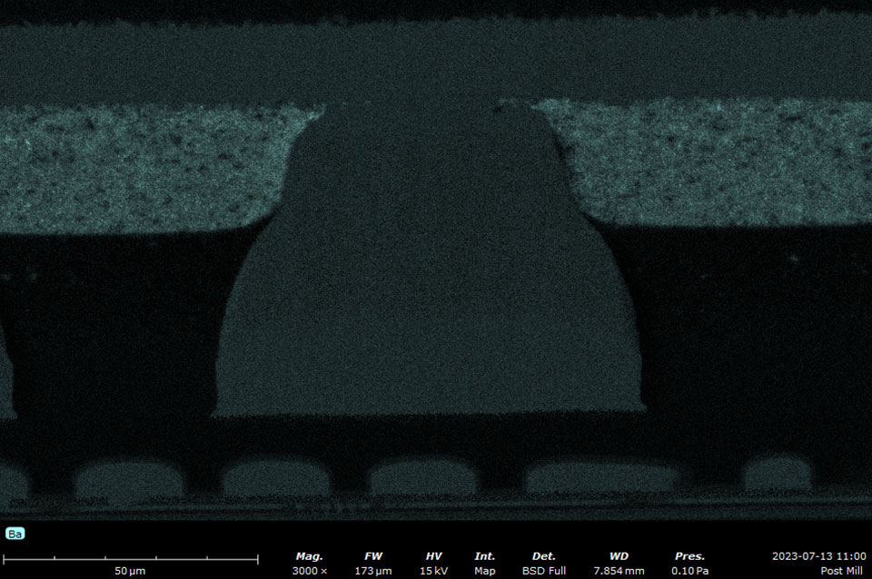
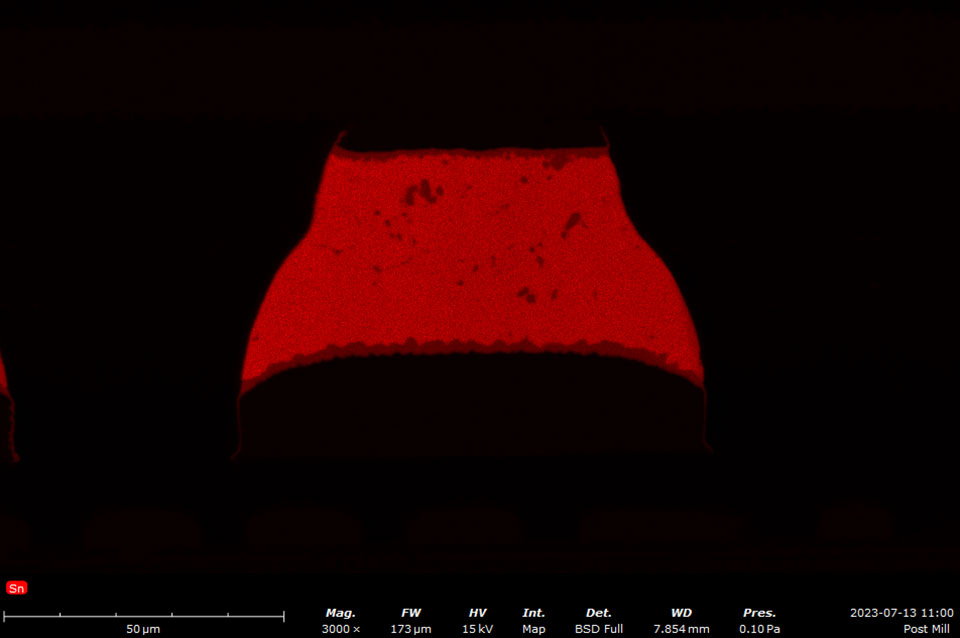
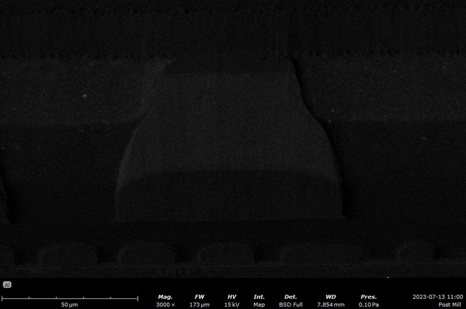
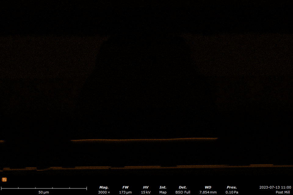
EDS makes use of the characteristic X-rays that are emitted from the sample during SEM imaging. It is a fast, accurate, and non-destructive method for identifying elemental composition on the micron scale. Characteristic X-rays are emitted when the electron beam displaces an inner shell electron (that belongs to an atom in the sample) that is replaced by an outer shell electron. Because each element has a unique energy difference between outer and inner electron shells, the X-rays that are detected are at specific energies that can be correlated with an elemental identification. EDS data can be obtained at a point, along with a line, or mapped over an area.
A silicon drift detector (SDD) is the most common type of EDS detector used in a SEM instrument. The SDD is composed of a solid-state sensor that generates electron-hole pairs by absorbing X-rays. By measuring the charge generated in the detector over a signal collection period, a spectrum of signal intensity vs. X-ray energy can be acquired allowing for the identification of almost all elements. Most SDDs contain a thin window, which provides a physical barrier for the detector to maintain appropriate vacuum levels while samples are being exchanged. The window allows all but low-energy X-rays to pass through, depending on the specific material and thickness. Beryllium windows are robust but do absorb X-rays from elements up to Be, meaning that elements from B and of higher atomic numbers can still be detected.
References
- D. B. Williams and C. B. Carter, Transmission Electron Microscopy, Springer, 2009. https://doi.org/10.1007/978-0-387-76501-3. ↩︎
- W. Zhou, R. Apkarian, Z. L. Wang and D. Joy, “Fundamentals of Scanning Electron Microscopy (SEM),” in Scanning Microscopy for Nanotechnology, Springer, 2007, pp. 1-40. https://doi.org/10.1007/978-0-387-39620-0_1. ↩︎
Scanning Electron Microscopy
Additional Resources:
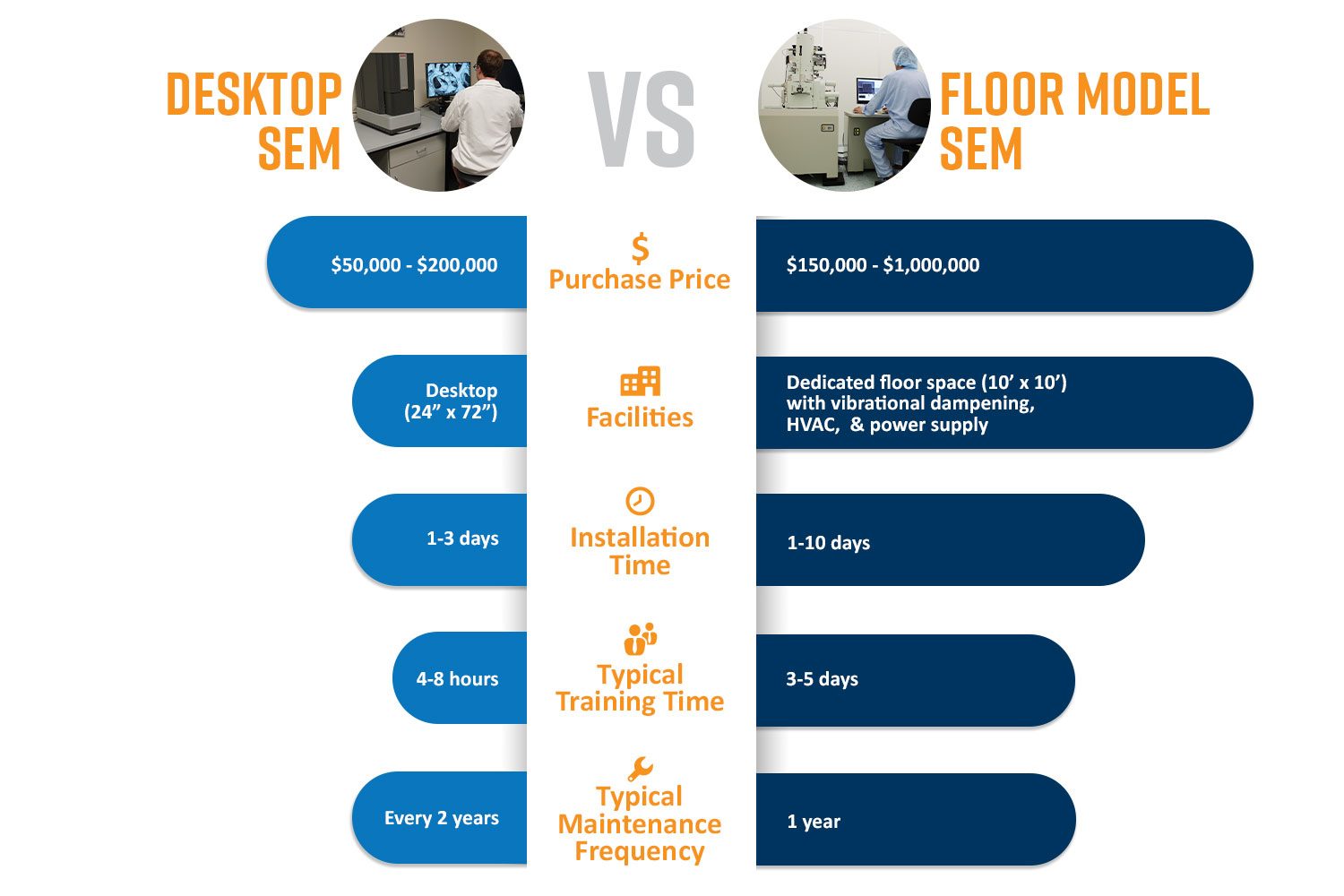
How Much Does a Scanning Electron Microscope (SEM) Cost?
A scanning electron microscope (SEM) is a powerful scientific instrument used for high-res…
8 Factors to Consider when Purchasing a Scanning Electron Microscope (SEM)
Purchasing a scanning electron microscope (SEM) can offer significant competitive advantag…
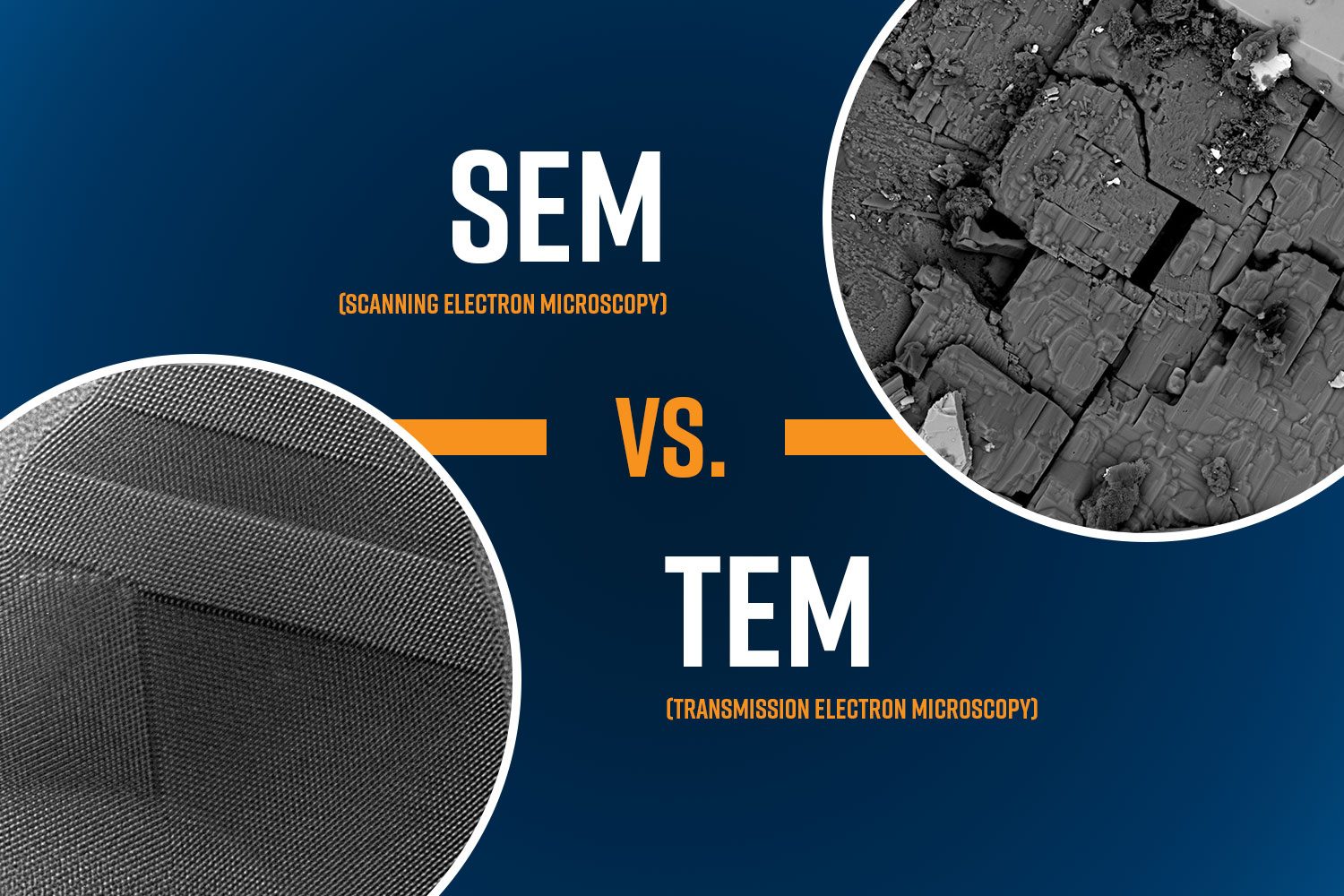
What’s the Difference Between SEM & TEM?
Electron microscopy is best known as a high-powered microscopy technique that utilizes a b…