Microscopy is a technique that allows us to visualize matter on length scales not visible to the human eye. Two of the most common microscopy techniques are optical microscopy (OM) and electron microscopy (EM). Each method is based on distinct principles with differing capabilities that can be leveraged for a broad spectrum of scientific disciplines such as biology, materials science, engineering, manufacturing, pharmaceutical R&D, forensics, and food science.
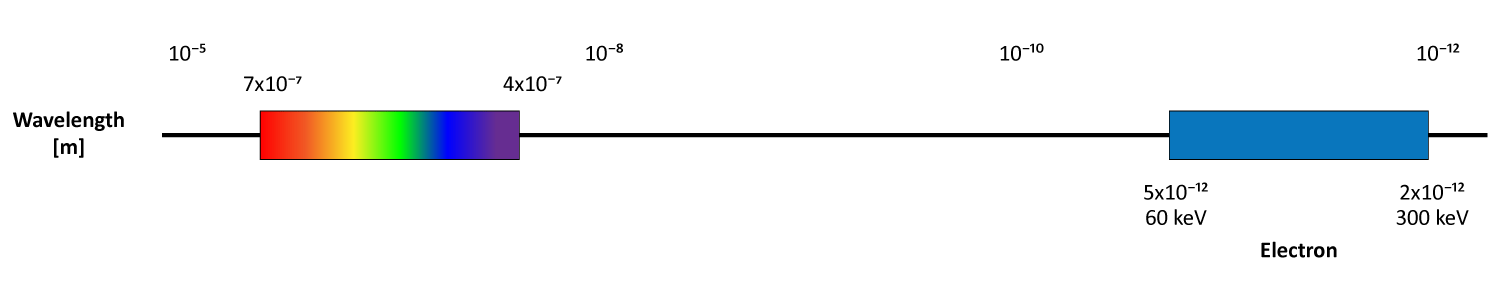
The main difference between optical and electron microscopy lies in the type of fundamental particle used in the microscope and its corresponding wavelength: OM uses visible light photons (400 – 700 nm), while EM employs a focused beam of electrons having wavelengths thousands of times smaller (pm). Electron microscopy offers much higher resolution and magnification compared to optical microscopy, allowing for the visualization of greater details in samples. This blog explores the theoretical and practical aspects of OM and EM while also demonstrating how the two techniques complement each other and expand our ability to visualize and analyze the world around us.

Optical Microscopy
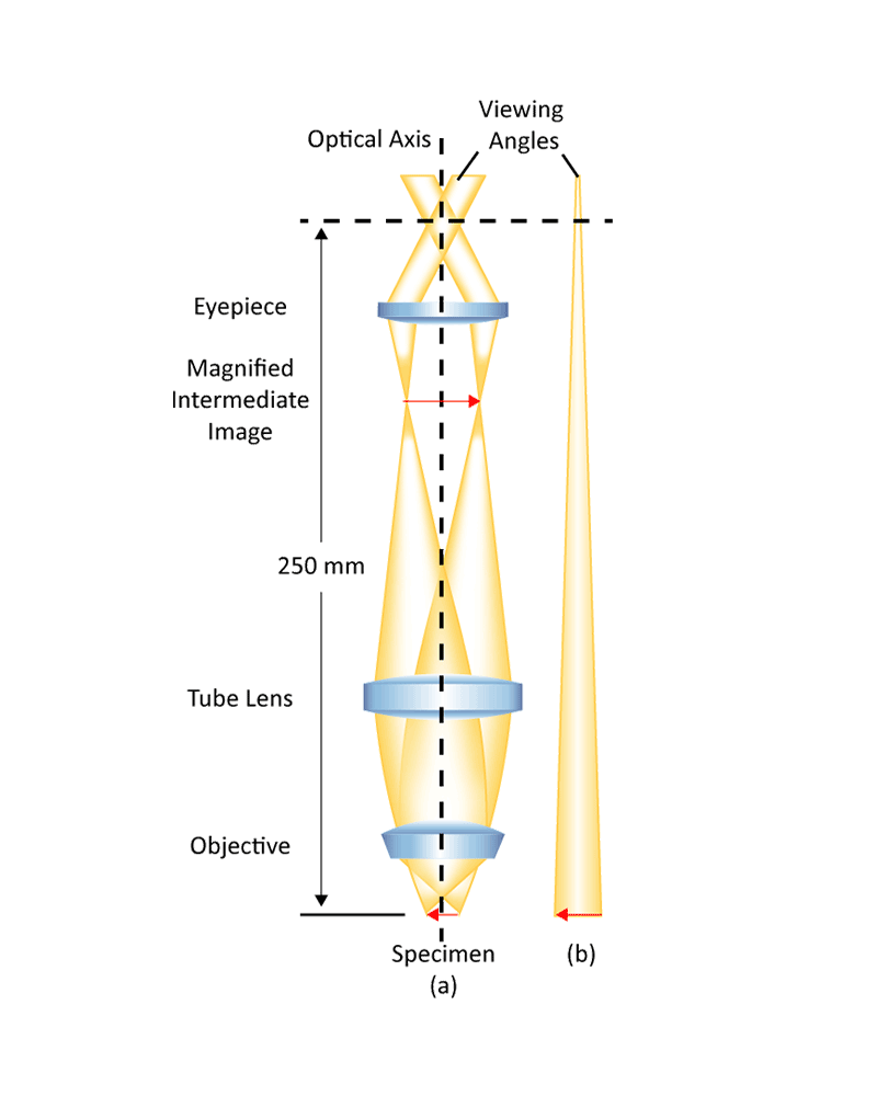
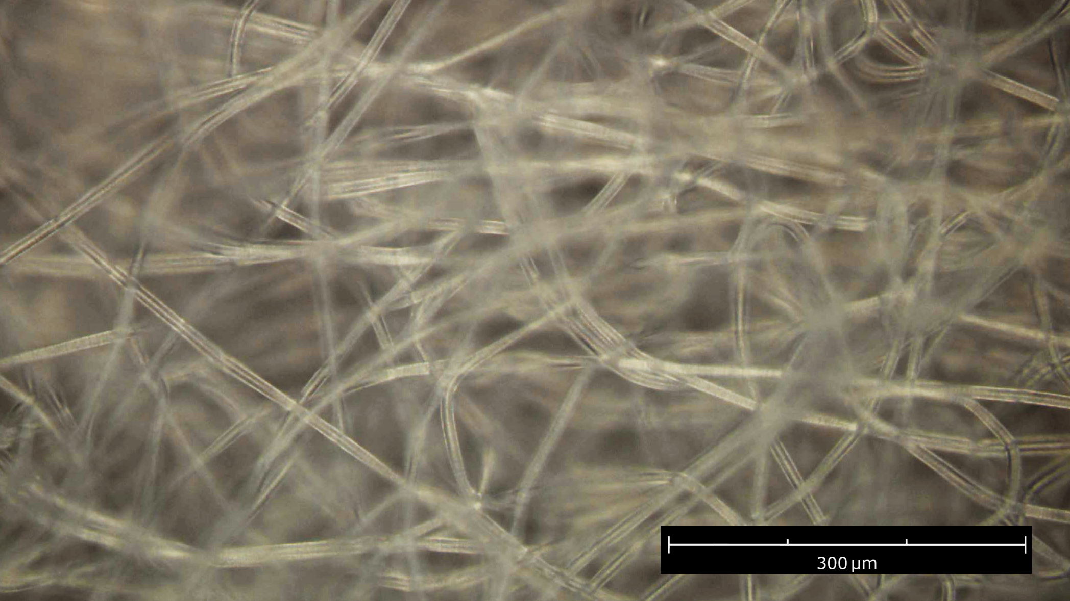
An optical microscope utilizes visible light and a series of lenses to generate a magnified image of an object. The sample is illuminated with visible light, which is then collected by the microscope’s objective lens and magnified through a series of additional lenses to create an image observable through an eyepiece or recordable by a camera (Figure 1). Optical microscopy is a versatile tool used across various scientific disciplines and industries. Optical microscopes are widely used in biology, materials science, forensics, and quality control and are ideal for observing larger structures, live samples, and fluorescently labeled materials.
Advantages of Optical Microscopes
Optical microscopes are widely available and relatively affordable, making them accessible to a broad range of users, from students in classrooms to researchers in laboratories. Sample preparation for optical microscopy is often simpler and less labor-intensive compared to electron microscopy. Optical microscopes can be configured for live imaging, allowing researchers to observe dynamic processes in real-time, such as cell division or microbial motility.
Limitations of Optical Microscopes
In an optical microscope, the incident light waves are bent around the object being imaged through a process known as diffraction. As the light waves spread out, they create an interference pattern with characteristic light and dark regions that are the basis for the image formed by the objective lens. According to the Rayleigh criterion, the diffraction-limited resolution of an optical microscope is approximately half the wavelength of the light used for imaging. For visible light (with wavelengths ranging from about 400 to 700 nanometers), the diffraction-limited resolution is typically around 200 to 350 nanometers.
Additionally, the relatively narrow depth of field in optical microscopy, which determines vertical range (i.e., along the optical axis) that can be sharply in focus simultaneously, can be a hindrance when examining large samples or those with complex three-dimensional structures. Also, achieving high contrast in optical microscopy can be difficult, especially with transparent or low-contrast specimens.
Beyond Optical Limits with Electron Microscopy
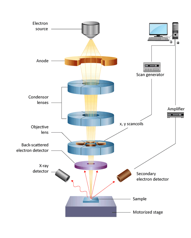
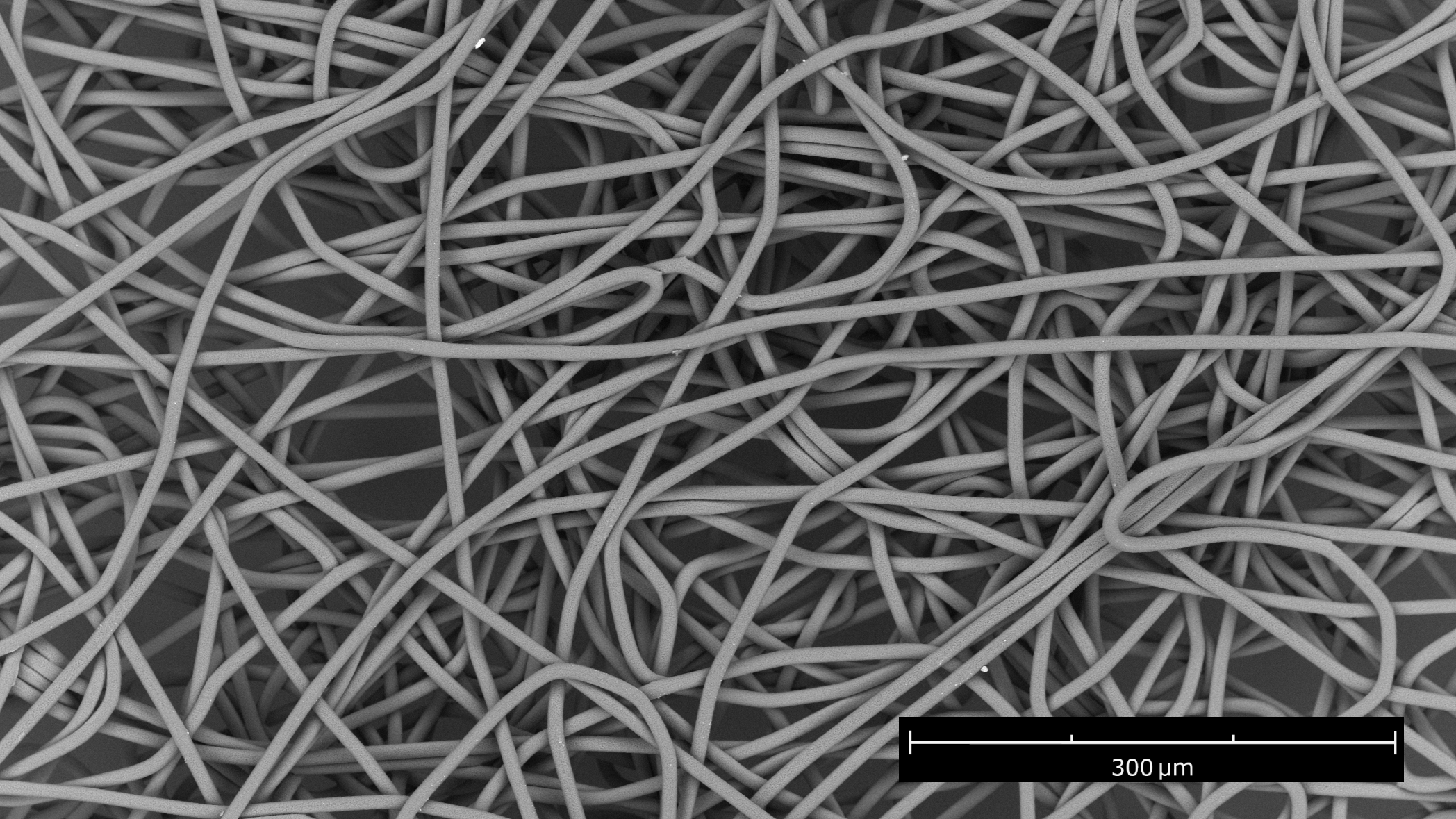
An electron microscope uses a beam of electrons to probe a sample and gain information about its structure and composition. The electron beam is either scanned across its surface, probing only the top layers in a mode called scanning electron microscopy (SEM), or is transmitted through a sample in a mode called transmission electron microscopy (TEM). What separates SEM and TEM is not only how the electron beam interacts with the samples but also the different signals that are generated and how the images are formed. The superior resolution and magnification due to the shift from photons to electrons reveals intricate details of surface topography that is not possible with optical microscopy. Electron microscopes are essential for studying nanomaterials, viruses, cellular ultrastructure, and single molecules. EM enables detailed imaging of subcellular organelles, nanomaterials characterization, and surface topography analysis.
Advantages of Electron Microscopes
Electron microscopes can achieve much higher resolution than optical microscopes, owing to the shorter wavelength of electrons. SEMs can achieve spatial resolutions ranging from <1 nanometers to 20 nanometers. The spatial resolution in a SEM is influenced by multiple factors including the spot size of the electron beam and volume of interaction with the sample. The accelerating voltage determines the kinetic energy, and wavelength, of the incident electrons, which influences the beam spot size and the depth of penetration of the electron beam within the sample. The volume of interaction also depends upon the density of the sample as well as the type of signal being analyzed. Compared to OM, SEM’s superior depth of field provides visualization of a specimen’s topology with remarkable depth perception (Figure 2).
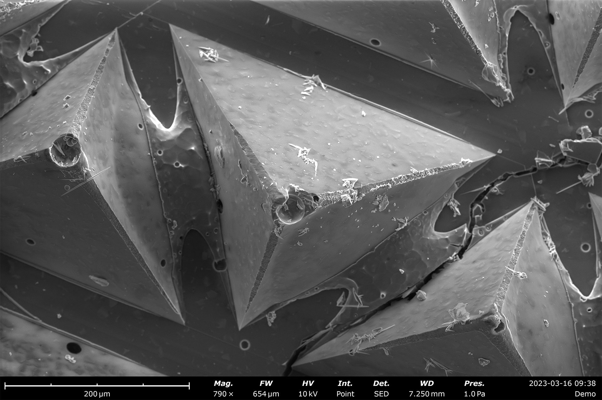
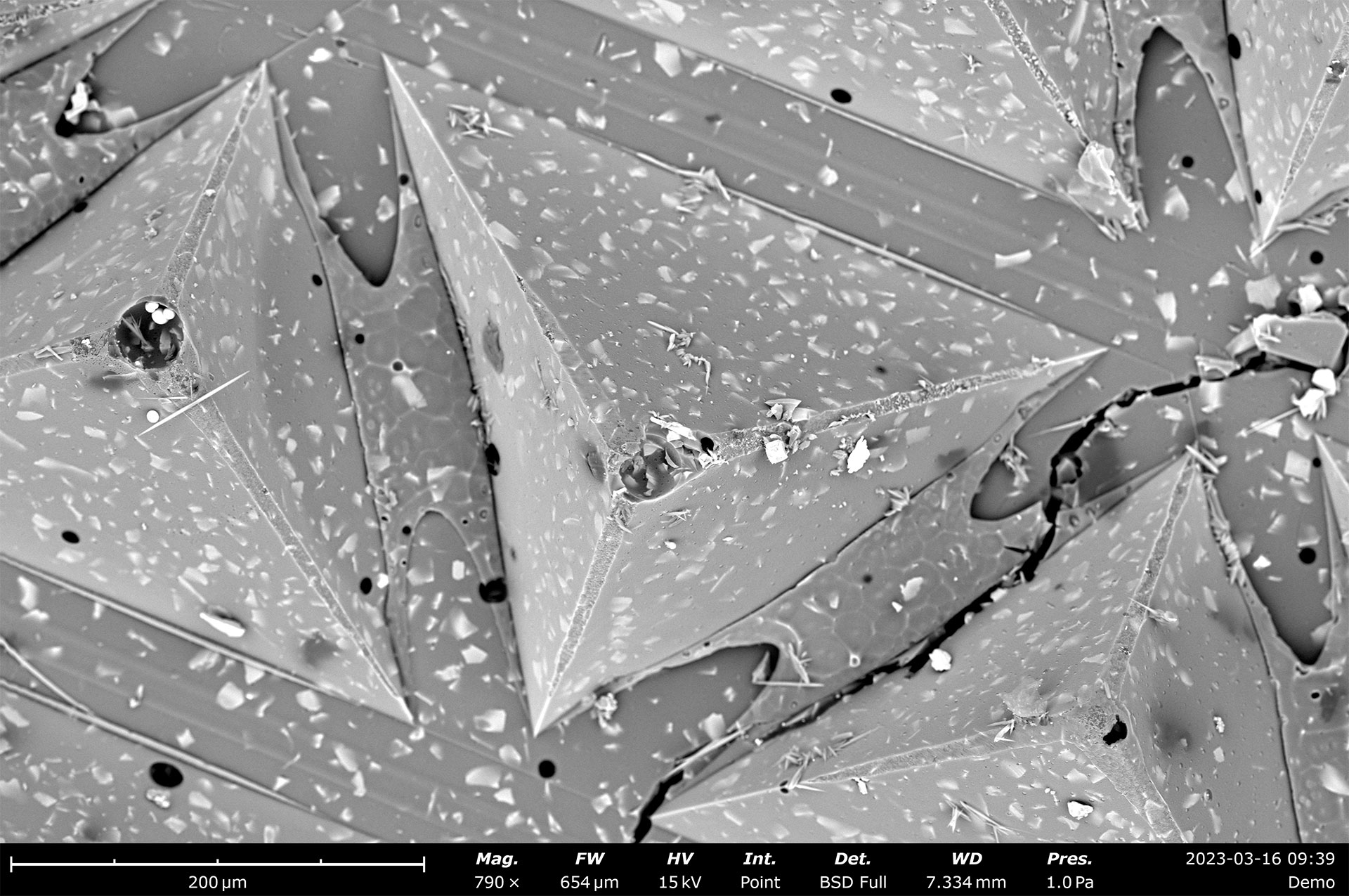
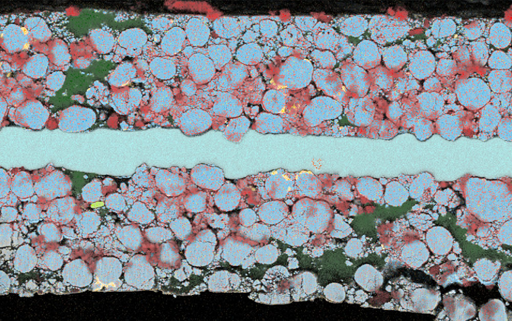
Electron microscopy techniques offer diverse imaging modalities, each suited to different types of samples and applications. For example, in an SEM, the backscattered electrons and secondary electrons generated during the interaction of the electron beam with the sample surface can be used to form high-resolution images of a sample’s surface topography and compositional differences, respectively (Figure 3). In addition, the characteristic X-rays emitted from a sample can be utilized to generate high resolution elemental maps of the surface (Figure 4).
Limitations of Electron Microscopes
Electron microscopes are complex instruments that require specialized training to operate and maintain. They are also considerably more expensive to purchase and maintain than optical microscopes. Sample preparation for electron microscopy typically involves extensive processing, including fixation, dehydration, and staining, which can introduce artifacts and alter sample morphology. Electron microscopes operate under vacuum conditions, which may limit the types of samples that can be imaged and require additional precautions for biological specimens.
Key Takeaways
The synergy between OM and SEM enriches our understanding of the microscopic world, connecting macroscopic observations to nanoscopic details. This integrated approach not only maximizes the investigative potential of both techniques but also drives forward scientific advancement across a multitude of disciplines. By understanding the strengths and limitations of each technique, researchers can choose the most appropriate tool for their specific applications.
- OM uses visible light and lenses to form a magnified image of a specimen and is usually a first-line option when tackling any microscopy application.
- OM encounters limitations in resolution and depth of field, prompting the need for more advanced methods.
- EM uses an electron beam to probe the sample, allowing for higher resolution images to be generated that reveal microstructural details not visible through OM.
- SEM provides the added opportunity to perform compositional mapping at the nanoscale through EDS.