What is Atomic Force Microscopy?
Since the introduction of the Nobel Prize-winning scanning tunneling microscope (STM) and then the invention of the atomic force microscopy (AFM) from the landmark publication by Binnig, Quate, and Gerber, the field of scanning probe microscopy has exploded well beyond using interatomic forces to image topography on the nanometer scale. The ability to measure intermolecular forces and see atoms is scientifically tantalizing.
Topography imaging alone does not always provide the answers that researchers need and the surface topology often does not correlate to the material properties. For these reasons, advanced imaging modes have been developed to provide quantitative data on a variety of surfaces. Now, many material properties can be determined with AFM techniques, including friction, electrical forces, capacitance, magnetic forces, conductivity, viscoelasticity, surface potential, and resistance.
Scanning Tunneling Microscopy
The development of the family of scanning probe microscopes started with the original invention of the STM in 1981. Gerd Binnig and Heinrich Rohrer developed the first working STM while working at IBM Zurich Research Laboratories in Switzerland. This instrument would later win Binnig and Rohrer the Nobel prize in physics in 1986.
Atomic Force Microscopy
The atomic force microscope (AFM) was developed to overcome a basic drawback with STM – it can only image conducting or semiconducting surfaces. The AFM has the advantage of imaging almost any type of surface, including polymers, ceramics, composites, glass, and biological samples.
Binnig, Quate, and Gerber invented the AFM in 1985. Their original AFM consisted of a diamond shard attached to a strip of gold foil. The diamond tip contacted the surface directly, with the interatomic van der Waals forces providing the interaction mechanism. Detection of the cantilever’s vertical movement was done with a second tip – an STM placed above the cantilever.
How an Atomic Force Microscope works
Analogous to how an Scanning Tunneling Microscope works, a sharp tip is raster-scanned over a surface using a feedback loop to adjust parameters needed to image a surface. Unlike Scanning Tunneling Microscopes, the Atomic Force Microscope does not need a conducting sample. Instead of using the quantum mechanical effect of tunneling, atomic forces are used to map the tip-sample interaction.
Often referred to as scanning probe microscopy (SPM), there are Atomic Force Microscopy techniques for almost any measurable force interaction – van der Waals, electrical, magnetic, thermal. For some of the more specialized techniques, modified tips and software adjustments are needed.
In addition to Angstrom-level positioning and feedback loop control, there are 2 components typically included in Atomic Force Microscopy: Deflection and Force Measurement.
AFM Probe Deflection
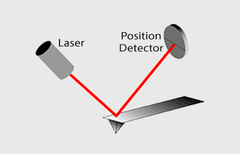
Traditionally, most Atomic Force Microscopes use a laser beam deflection system where a laser is reflected from the back of the reflective AFM lever and onto a position-sensitive detector. AFM tips and cantilevers are typically micro-fabricated from Si or Si3N4. Typical tip radius is from a few to 10s of nm.
Measuring Forces
Because the Atomic Force Microscope relies on the forces between the tip and sample, these forces impact AFM imaging. The force is not measured directly, but calculated by measuring the deflection of the lever, knowing the stiffness of the cantilever.
Hooke’s law gives:
F = -kz
where F is the force, k is the stiffness of the lever, and z is the distance the lever is bent.
Feedback Loop for Atomic Force Microscopy
Atomic Force Microscopy has a feedback loop using the laser deflection to control the force and tip position. As shown, a laser is reflected from the back of a cantilever that includes the AFM tip. As the tip interacts with the surface, the laser position on the photodetector is used in the feedback loop to track the surface for imaging and measuring.
Contact Modes for AFM
Contact Mode
The first and original mode of operation is contact mode. As the tip is raster-scanned across the surface, the lever is deflected as it moves over the surface topography.
There are two methods of imaging in contact mode: constant force or constant height. In constant force mode, the tip is continually adjusted to maintain a specified deflection. It is this adjustment that is used to display an image.
When the tip scans in constant height mode, the sample must be relatively flat for the feedback loop to maintain control during scanning. This is useful for small, high-speed atomic resolution scans.
Because the tip is in hard contact with the surface, the stiffness of the lever needs to be less that the effective spring constant holding atoms together, which is on the order of 1 – 10 nN/nm. Most contact mode levers have a spring constant less than 1 N/m.
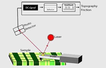
Friction Force Mode
Also known as friction force mode, Lateral Force Microscopy (LFM) measures frictional forces on a surface. By measuring the lateral twist of the cantilever, rather than its deflection, areas of higher and lower friction are imaged.
Dynamic Modes for AFM
Non-Contact Mode
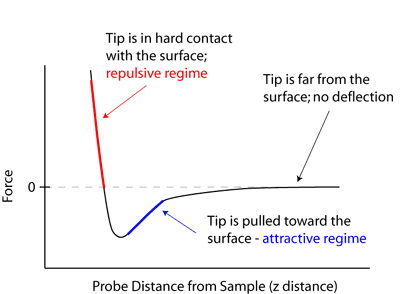
Non-contact mode belongs to a family of AC modes, which refers to the use of an oscillating cantilever. A stiff cantilever is oscillated in the attractive regime, meaning that the tip is quite close to the sample, but not touching it (hence, non-contact). The forces between the tip and sample are quite low, on the order of pN (10-12 N). The detection scheme is based on measuring changes to the resonant frequency or amplitude of the cantilever as the interaction between the tip and sample dampen the oscillation.
Dynamic Force Mode
Also known as tapping mode, intermittent-contact mode, acoustic AC mode or oscillating mode.
A stiff cantilever is oscillated closer to the sample than in noncontact mode. Part of the oscillation extends into the repulsive regime, so the tip intermittently touches or taps the surface. Very stiff cantilevers are typically used, as tips can get stuck in the water contamination layer.
The advantage of tapping the surface is improved lateral resolution on soft samples. Lateral forces such as drag, common in contact mode, are virtually eliminated. For poorly adsorbed specimens on a substrate surface, the advantage is clearly seen.
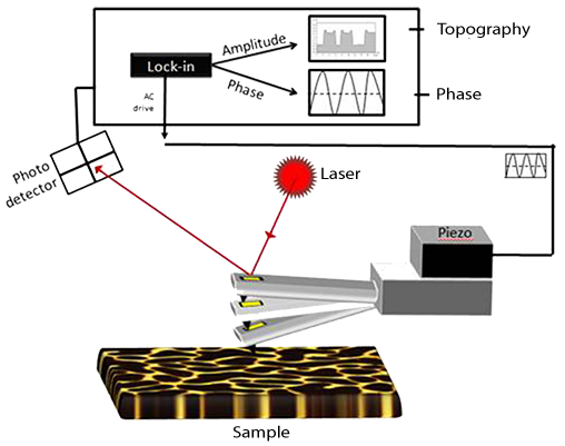
Phase Contrast
In Phase Contrast mode, the phase shift of the oscillating cantilever relative to the driving signal is measured. This phase shift can be correlated with specific material properties that effect the tip/sample interaction. The phase shift can be used to differentiate areas on a sample with such differing properties as friction, adhesion and viscoelasticity. The technique is used simultaneously with DFM mode so topography can be measured as well.
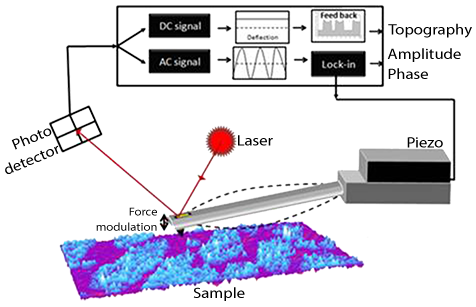
Force Modulation
Force modulation refers to a method used to probe properties of materials through sample/tip interactions. The tip (or sample) is oscillated at a high frequency and pushed into the repulsive regime. The slope of the force-distance curve is measured which is correlated to the sample’s elasticity. The data can be acquired along with topography which allows comparison of height and material properties.
Electrical Modes for AFM
Electric Force Microscopy
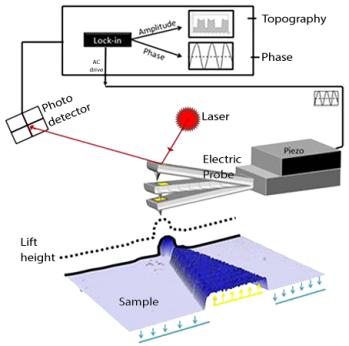
EFM oscillates a conducting AFM tip to sense electric force gradients. Usually, this is done in 2 passes – one to measure the topography in a standard dynamic mode and the second to “lift” a set amount above the recorded profile to measure electric field strength. Using the phase signal, a map of the gradient of the electric field is created.
Kelvin Probe Force Microscopy
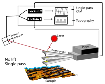
Like EFM, KFM also is an oscillating technique that requires a conducting probe. Kelvin Probe Force Microscopy (KFM) mode measures the work function of the surface. It is also known as surface potential microscopy.
This mode can be done as a lift technique (dual pass) or as a single-pass method. The single-pass method, referred to as High Definition KFM (HD KFM), offers higher sensitivity for measuring the surface potential plus higher spatial resolution. HD KFM requires a second lock-in amplifier as shown below. Because the single pass does not require tip to “lift” above the surface, resolution of the electrical signal is much stronger and provides the added resolution.
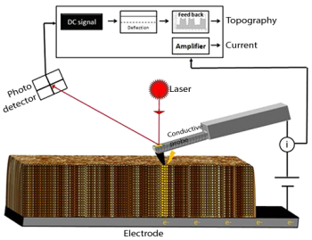
Conductive AFM
Conducting AFM, or Scanning Spreadding Resistance (SSR), is used to image a material in contact mode with a conductive AFM tip. By biasing the tip (or sample) the current is measured passing from one to the other and a map ofthe conductivity (or inversely, resistivity) can be obtained.
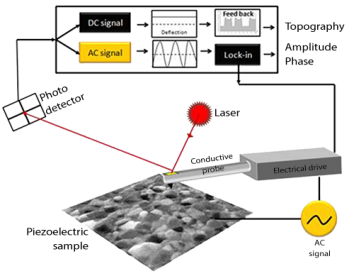
Piezoresponse Force Microscopy
Piezoresponse Force Microscopy (PFM) mode is a Contact mode technique that maps piezoelectric domains. PFM uses the inverse piezoelectric effect by applying a voltage to use the resulting deformation in the material to map the piezoelectrical properties of a surface. This method requires a conductive probe and an applied AC signal. The amplitude and phase signals are used to measure piezoelectric orientation.