
243rd ECS Meeting Find us the Exhibit Hall and discover our suite of electrochemistry solutions designed to empower your battery research. Explore structure-activity relationships with…
Posted: May 12, 2023

“We discovered Phenom has the best value with results close to a full-size SEM” – Dr Naomi C., Menlo Micro On occasion, we are given…
Posted: May 10, 2023
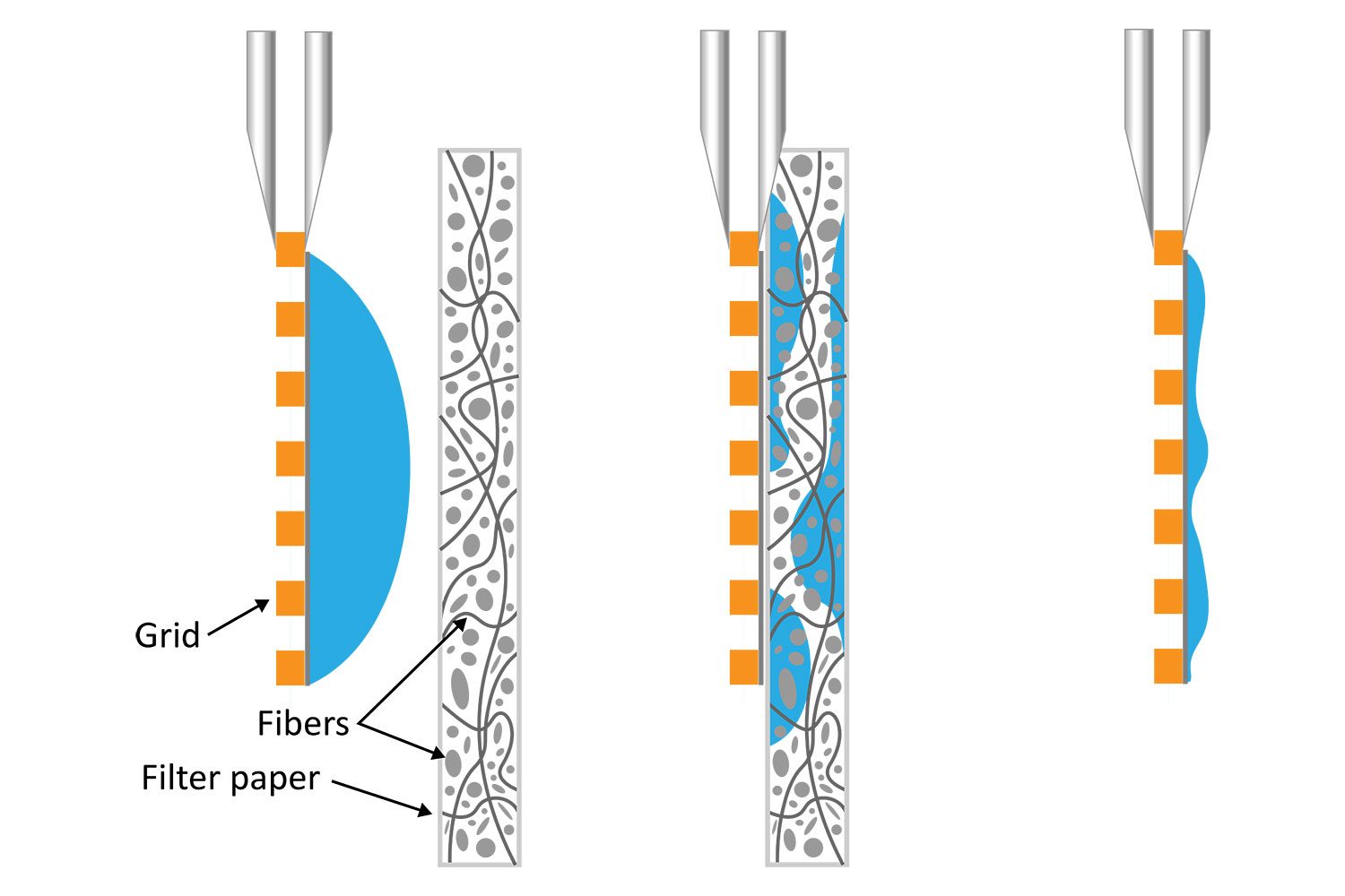
The air-water interface (AWI) is essentially the chaotic boundary where a solution meets the air. When protein molecules in solution contact the AWI, they tend…
Posted: May 3, 2023
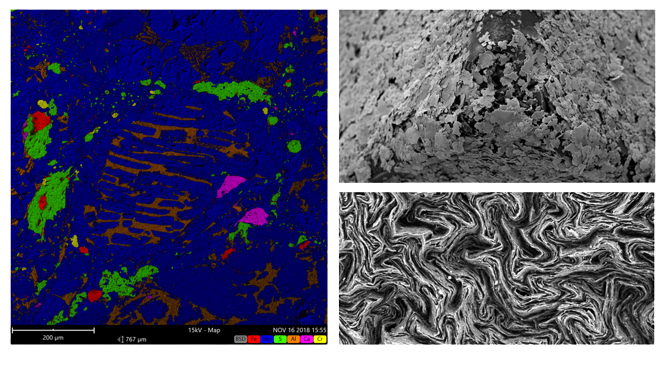
Scanning electron microscopy (SEM) is an extremely versatile analytical technique that produces high-resolution images by scanning a focused electron beam across a sample surface. Within…
Posted: April 19, 2023
We would like to invite you to our upcoming open house event on Wednesday, May 10th, taking place at our Alexandria, VA office near Washington…
Posted: April 11, 2023

Society for Biomaterials Annual Meeting & Exposition “Riding the Translational Waves to the Future” Find us at the expo to explore our solutions for biomaterials…
Posted: April 6, 2023
We are pleased to invite you to an exciting event showcasing the latest advances in scanning electron microscopy (SEM) along with FT-IR and Raman spectroscopy….
Posted: March 30, 2023
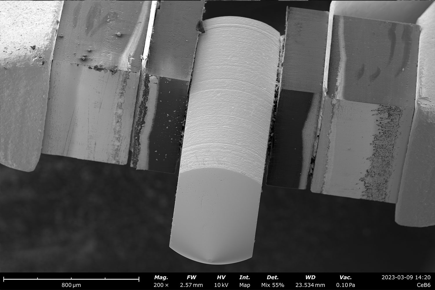
The electron source is one of the most important components of a scanning electron microscope (SEM) and is a major factor in determining its maximum…
Posted: March 28, 2023
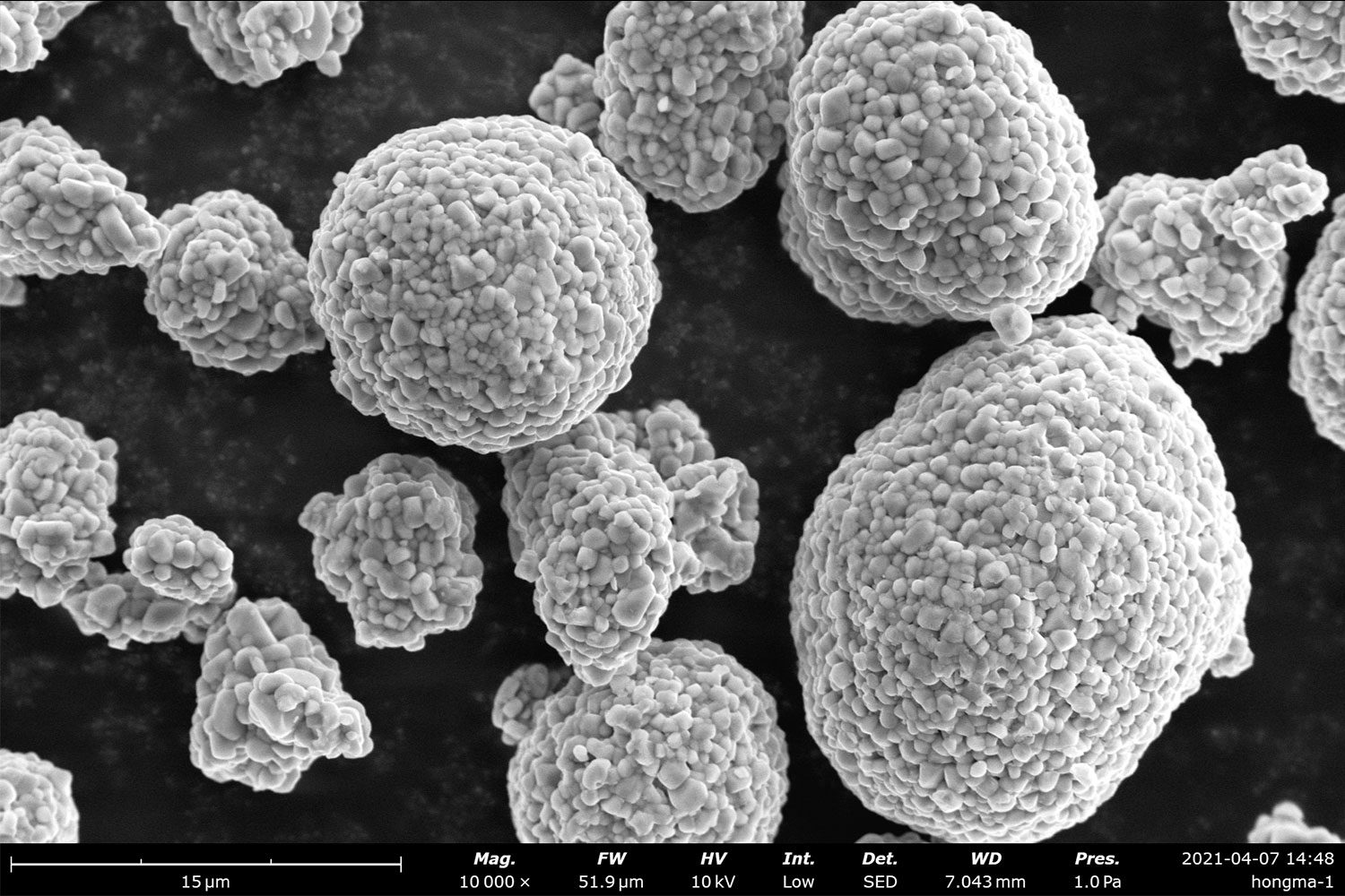
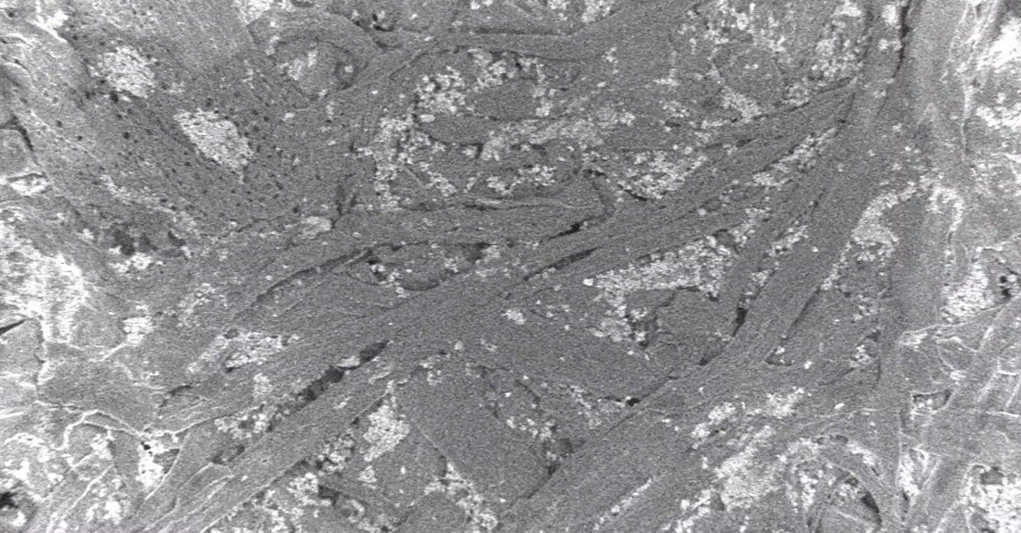
The functional properties of a battery, not limited to just its performance, are inherently dependent upon the microstructure and surface morphology of electrodes and separators….
Posted: February 22, 2023
CERES Ice Shield METEOR VitroJet Stream FAST-EM Biophysical Society Annual Meeting 2023 Join us February 19-21, 2023Sunday, Feb 19 | 10:00AM – 5:00PMMonday, Feb 20…
Posted: February 19, 2023
You’re invited to experience scanning electron microscopy firsthand with the Phenom Desktop SEM, guided by our own experts in live demo sessions and provided with…
Posted: February 14, 2023
The fundamental unit of electric charge is the electron, an elementary particle that can be used in the domain of microscopy to see beyond the…
Posted: February 8, 2023
Copyright 2024. Nanoscience Instruments. All Rights Reserved.
This site is protected by reCAPTCHA and the Google Privacy Policy and Terms of Service apply.